What if diamonds could power the next generation of electronics?
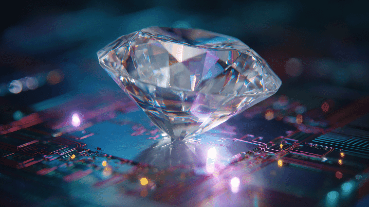
Not as jewelry, but as the "ultimate semiconductor material," with thermal conductivity 13 times greater than silicon, voltage resistance 30 times higher, and the ability to function in extreme environments from deep space to nuclear reactors.
Japan's HORIBA, a Kyoto-based precision measurement giant, just made a strategic move to turn this vision into reality by acquiring an Indian lab-grown diamond startup.
A Kyoto Measurement Giant Bets on Diamonds
In February 2026, HORIBA India, a subsidiary of HORIBA, Ltd. (headquartered in Kyoto), completed the acquisition of all shares in Pristine Deeptech Private Limited, a research-driven startup based in Gujarat, India. The deal, reported to be worth several million dollars, was finalized on January 14, 2026.
HORIBA is a global leader in analytical and measurement instruments, founded in 1945 by Masao Horiba, a nuclear physics student at Kyoto University. The company holds approximately 80% of the global market share for automotive exhaust gas analyzers and operates across five key sectors: automotive testing, environmental monitoring, medical diagnostics, semiconductor manufacturing, and scientific research. With over 8,900 employees across roughly 50 companies in 29 countries, HORIBA is quietly one of Japan's most globally influential technology firms.
So why would a precision measurement company acquire a diamond startup?
Why Diamonds Are the "Ultimate Semiconductor"
To understand this move, you need to understand why lab-grown diamonds are generating so much excitement in the semiconductor industry.
Today's electronics rely overwhelmingly on silicon-based chips. But as devices push toward higher power, higher frequencies, and harsher operating environments, silicon is hitting its physical limits. Next-generation materials like silicon carbide (SiC) and gallium nitride (GaN) have emerged as alternatives, but diamond stands in a class entirely by itself.
Diamond's advantages as a semiconductor material are staggering. Its thermal conductivity is roughly 13 times that of silicon, meaning it can dissipate heat far more efficiently, a critical factor as AI chips and EV power electronics generate ever more heat. Its dielectric breakdown voltage is about 30 times higher than silicon, enabling operation at extreme voltages. And its electron mobility allows for high-frequency operation that could revolutionize communications technology.
These properties make diamond semiconductors ideal candidates for next-generation power devices in electric vehicles, 5G/6G communications infrastructure, data centers, space and defense applications, and quantum sensors that can measure magnetic fields and temperatures with unprecedented precision.
The catch? Diamond is the hardest known material, making it exceptionally difficult to cut, polish, and process into semiconductor wafers. The technology to grow large, high-quality synthetic diamond crystals and fabricate them into working devices has been one of the great engineering challenges of the semiconductor world.
Pristine Deeptech: A Small Team with Big Expertise
Pristine Deeptech, founded in October 2021 in Gujarat's emerging tech ecosystem, is a compact but specialized operation, with just seven employees focused entirely on lab-grown diamond R&D. Despite its small size, the startup has built end-to-end capabilities, from diamond research to the development and sale of MPCVD (Microwave Plasma Chemical Vapor Deposition) equipment, the key manufacturing technology for growing synthetic diamond crystals.
MPCVD works by using microwave energy to create a plasma that breaks down carbon-containing gases (like methane) and deposits diamond film onto a substrate, atom by atom. This process is how high-quality lab-grown diamonds are produced for both industrial and potential semiconductor applications.
HORIBA and Pristine Deeptech have had a business relationship since 2023, giving HORIBA time to evaluate the startup's capabilities before committing to full acquisition.
HORIBA's Three-Pronged Strategy
Following the acquisition, HORIBA has outlined three strategic pillars for leveraging its new diamond capabilities.
The first pillar is creating new analytical and measurement solutions for advanced materials. By combining Pristine Deeptech's diamond knowledge with HORIBA's established technologies, particularly Raman spectroscopy and other analytical tools, the company plans to develop measurement solutions that support the commercialization of diamond wafers and other advanced materials.
The second pillar involves developing diamond-based components and products. HORIBA intends to develop sensors and other components made from diamond, both for integration into HORIBA's own instruments (improving their performance) and for standalone sale as components.
The third pillar positions India as a core R&D hub. HORIBA sees India as a future global innovation center and plans to invest strategically in building HORIBA India into a leading R&D facility for advanced materials and semiconductor business. This aligns with India's rapidly growing role in the global semiconductor supply chain.
India as a Strategic Choice
The choice of India is no accident. HORIBA has been building its global R&D network since the 1990s, with facilities in France, the United States, and the United Kingdom. India, with its growing pool of engineering talent, expanding industrial base, and increasing government investment in semiconductor manufacturing, represents the next frontier.
Gujarat, where Pristine Deeptech is based, is also home to India's broader ambitions in semiconductor manufacturing, with major fab projects under development. By establishing a diamond-focused R&D presence in this ecosystem, HORIBA positions itself at the intersection of India's semiconductor aspirations and the global race toward next-generation materials.
The Bigger Picture: Japan's Diamond Semiconductor Race
HORIBA's acquisition fits into a broader Japanese push toward diamond semiconductor technology. Japan has emerged as a global leader in diamond semiconductor research, with several notable developments.
Okuma Diamond Device, a startup born from Hokkaido University and Japan's National Institute of Advanced Industrial Science and Technology (AIST), raised over $45 million and is building the world's first diamond semiconductor factory in Okuma-cho, Fukushima Prefecture, with operations planned for 2026. The factory specifically targets radiation-resistant semiconductors for use in the decommissioning of the Fukushima Daiichi Nuclear Power Plant.
Power Diamond Systems, based on research from Waseda University, is developing diamond power MOSFETs and has begun collaboration with JAXA for space applications. In 2023, a research team at Saga University achieved a breakthrough in developing the world's first diamond semiconductor power circuit, demonstrating switching operation.
The global diamond substrate market was valued at approximately $190 million in 2024 and is projected to reach around $260 million by 2030. While still small compared to silicon, the wider power semiconductor market is expected to reach approximately $59.6 billion by 2030, with diamond potentially capturing a growing share as manufacturing challenges are overcome.
What This Means for the Future
HORIBA's acquisition of Pristine Deeptech may seem modest in scale: a seven-person startup acquired for several million dollars. But it represents something significant: a measured, strategic bet by a globally respected Japanese instrument maker on what many consider the future of semiconductor materials.
By combining India's growing engineering ecosystem with Japan's measurement expertise and the emerging science of synthetic diamond semiconductors, HORIBA is positioning itself not just to analyze the next generation of materials, but to help create them.
The road from lab-grown diamond to practical diamond semiconductors is still long, and industry experts suggest widespread commercialization may be 10 to 15 years away. But with companies like HORIBA making strategic moves now, and Japanese researchers continuing to achieve breakthroughs, the era of diamond electronics may arrive sooner than many expect.
In Japan, there's growing excitement about diamond semiconductors as a potential arena where Japanese companies and researchers can lead globally. The country's strength in materials science and precision manufacturing gives it a natural advantage in this emerging field.
What about in your country? Is there research or industry interest in diamond semiconductors or other next-generation materials? Do you think lab-grown diamonds will eventually become as important to electronics as silicon is today? We'd love to hear your perspective.
References
- https://www.horiba.com/jpn/company/news/detail/news/2/2026/20260203-pd-jp/
- https://eetimes.itmedia.co.jp/ee/articles/2602/05/news038.html
- https://response.jp/article/2026/02/05/407006.html
- https://www.nikkei.com/article/DGXZQOUF034BN0T00C26A2000000/
- https://www.aist.go.jp/aist_j/magazine/20250326.html
- https://www.projectdesign.jp/articles/news/b69a88d6-1c90-49df-8be4-1cbbc5b0573b


Global Discussion
15 comments