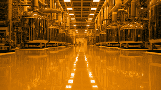
TOK has finished a 23-billion-yen photoresist building in Koriyama. Its 2023 and 2026 releases mention neither AI nor capacity; its earnings documents show how demand and the start date shifted in between.
Some AI GPUs are now far weaker at the FP64 math science needs. A Shibaura Institute of Technology method rebuilds it from low-precision units; NVIDIA lists up to 175 TFLOPS on a B200. How it works, and its limits.
Kanazawa University and AIST report the first vertical diamond MOSFET with an inversion-layer channel. Diamond transistors that switch off this way existed by 2016; what is new is building one vertically.
ABLIC's CLEAN-Boost banks tiny amounts of ambient energy and releases them in one burst, amplified up to 30,000 times. Inside the battery-less sensor that trips on 150 microliters of water.
Hafnium keeps advanced chips and jet engines running, yet the world makes about 71 tonnes a year, nearly all of it in France and the United States. An Osaka chemical maker now wants a share of it by 2028.
Navitas sued Renesas on August 10, 2026 over four US patents covering SuperGaN. The CEO who filed it once ran that business inside Renesas, which sued first over trade secrets and holds 39.9 percent of Wolfspeed.
Sony and TSMC signed a binding deal on August 11 to build smartphone image sensors in Kumamoto, contributing about 747 billion yen ($4.7 billion) toward production in 2029. TSMC takes only 38% and lets Sony lead.
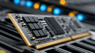
Kioxia's XL1 module pulls flash memory into the memory hierarchy over CXL to ease the DRAM crunch in AI data centers. What it can and cannot do, and why it matters for a country that no longer makes DRAM.
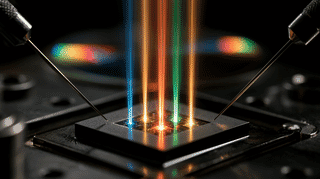
A terbium-doped AlGaN LED from the University of Osaka and Ritsumeikan University emits four colors from a single spot, with wavelengths that barely move as the current rises.
The July 28, 2026 Kumamoto earthquake hit shindo 7 and stopped chip plants run by Renesas, Sony, Mitsubishi Electric, TSMC's JASM and Tokyo Electron. The fab the world watched was not the real chokepoint: a coater/developer plant with roughly 90 percent of the world market was.
Resonac, BEAM and Nippon LEO signed an MOU to manufacture compound semiconductors in low Earth orbit. Why build chips in microgravity, and how Japan's bet compares to the US and China.
Japan's government just promised over 370 trillion yen ($2.3 trillion) across 17 strategic sectors by 2040. We unpack the suspicious arithmetic: a 6.5x return promised on chips, an undisclosed public-private split, and a deadline conveniently 14 years away.
Glass is the front-runner for AI chip packaging substrates, but its smooth surface won't hold wiring. Nikon's new PAP material uses light to solve it. A look at the hidden Japanese chokepoints in the chip-substrate supply chain.
Tokyo's Orbray and De Beers' Element Six have established a reproducible process for one of the largest single-crystal diamond wafers yet, at three inches. How a sapphire trick beat the cracking problem that long held back diamond, the material many call the ultimate semiconductor.
TSMC, the world's largest foundry, is quitting GaN power-chip manufacturing. ROHM, which built its flagship 650V parts inside TSMC's fabs, has licensed the technology and is racing to mass-produce in Hamamatsu by 2027. A look at the China-US rivalry and Japan's vertical-integration bet.
RIKEN and Enplas drill 1.1-micron, aspect-ratio-1,000 holes through glass in under a nanosecond, hitting 3,000 holes a second. As the chip race shifts from shrinking to packaging, here's why glass through-glass vias matter, and where Japan's materials and equipment makers fit.
A Japan-US team from Tohoku University and the US NIST built the first working spintronics probabilistic bit (P-bit) on a single silicon substrate using standard chip-fabrication processes. We explain the coin-flip idea, how it differs from quantum computing (room temperature, existing chip lines), and how far it really is from a product.
Sony Semiconductor Solutions is mass-producing the IMX711, a direct-conversion X-ray CMOS image sensor based on a pixel structure invented at Japan's RIKEN institute. With an industry-fastest 26,100fps and noise low enough to measure single X-ray photons, it ends a decades-old trade-off in X-ray imaging. Here's why battery makers, chip fabs and scientists are paying attention.
A ball bearing with a 0.6mm bore, smaller than a sesame seed. One firm in a former coal town in Hokkaido reportedly makes around 70% of the world's sub-millimeter bearings. Here's how.
Tokyo Ohka Kogyo is No. 1 in photoresist with a 24.7% share and No. 2 in EUV resist with 28%. How a 1936 maker of coal-lamp battery material became a chokepoint in the AI chip supply chain.