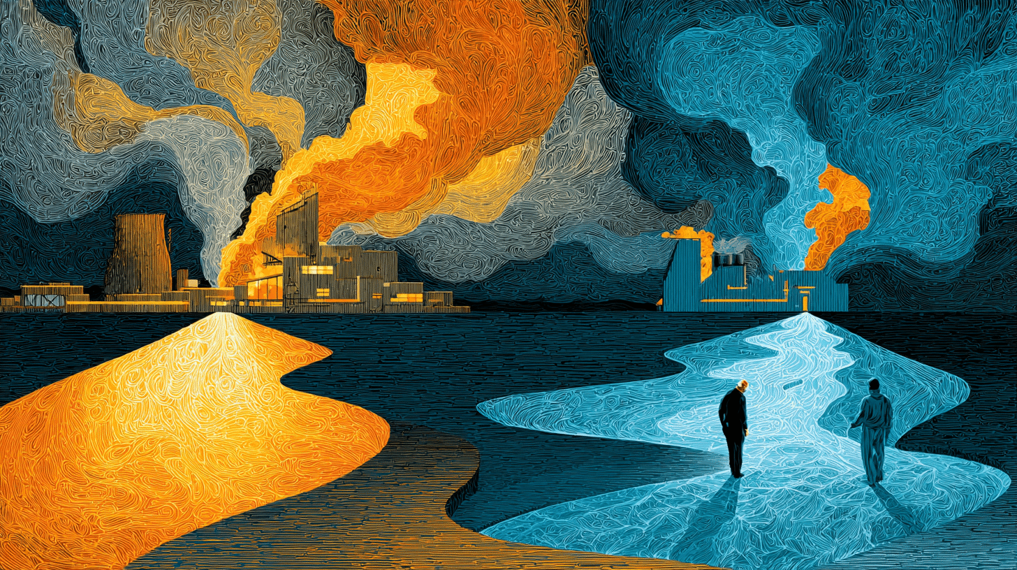
🔬 In late 2025, two of the biggest names in chipmaking quietly split on how to build the next generation of chips. In December, Intel announced it had installed and accepted the industry's first production-grade "High-NA" EUV machine, ASML's TWINSCAN EXE:5200B, at roughly $400 million a unit. TSMC bought one too, but decided against putting it on a production line for now. It intends to reach the 1.4-nanometer and 1-nanometer generations without it.
Fighting at the bleeding edge without the most advanced machine on the market sounds reckless. And there's an awkward piece of history that makes it sound even more so.
We've seen this movie before, and Intel was the one who lost
A decade ago, the company betting against the newest lithography wasn't TSMC. It was Intel.
In the mid-2010s Intel was still the undisputed king of chip manufacturing. Moving to its 10nm generation, it chose to stretch the older DUV (deep ultraviolet) light it already had, using elaborate multi-patterning tricks, rather than rush to adopt the new and unproven EUV. The gamble went badly. Yields were poor, and 10nm slipped year after year, by some accounts close to four years late.
Meanwhile TSMC and Samsung leaned hard into EUV at their 7nm and 5nm nodes. By 2020, around half of all the EUV machines in the world were installed in TSMC's fabs while Intel had barely begun using the technology, a bitter irony given that Intel itself had helped fund EUV's early development. By the time Intel shipped 10nm in volume, TSMC had already sold huge quantities of more advanced chips and won the trust of Apple, AMD and Nvidia. Many analysts concluded Intel had lost its process crown for good.
Intel says it won't make that mistake twice. It was the first customer to take ASML's R&D-grade EXE:5000 back in 2023, and the first to install the production-grade EXE:5200B. Its 14A node is slated for risk production in 2027 and volume manufacturing in 2028. That is precisely Intel refusing to be late to the newest tool again.
Which is what makes TSMC's decision so striking. Stretching an older machine instead of adopting the new one is, almost exactly, the move that cost Intel a decade. So is TSMC walking into the same trap?
TSMC's bet: skip the $400 million machine, on purpose
TSMC's leaders insist it isn't a trap. At the company's shareholder meeting on June 4, 2026, chairman C.C. Wei confirmed TSMC has bought a High-NA machine, but only for research, with no plans to use it in mass production yet, purely, he said, because of cost. "When costs come down and we can fully leverage their benefits, we will introduce them to production," he added. Reports suggest TSMC means to keep squeezing its existing EUV machines through 1.4nm and 1nm, perhaps until around 2029.
The logic is real. A High-NA machine prints the finest features in a single, sharp exposure; an older machine has to split the same pattern across several exposures (multi-patterning), which means more steps, more masks and more cost per layer. But each High-NA tool costs roughly $400 million, and TSMC is betting that pushing its cheaper machines a little further is the smarter economics, even if it's the harder engineering.
It's a genuine gamble. If multi-patterning gets too costly or too error-prone at 1nm, Intel's expensive head start could pay off. So the obvious question is: what gives TSMC the confidence to take the same kind of bet that once buried Intel?
TSMC's confidence rests on a thin Japanese film
Part of the answer is a component most people have never heard of, and a Japanese company that quietly owns it.
To push an older EUV machine to ever-smaller features, you cannot afford a single stray particle landing on the mask, because at these dimensions one speck prints as a fatal defect. The shield against that is the pellicle: a thin, transparent membrane stretched over the photomask like a dust cover. On EUV machines it is fiendishly hard to make, because the film has to let EUV light pass through while surviving an intense beam that can heat the mask toward 1,000°C. The harder TSMC works its older machines, the more it leans on pellicle performance to hold yields up.
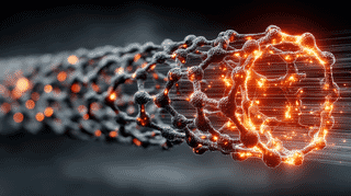
The pioneer here is Japan's Mitsui Chemicals, which has made pellicles since 1984. It licensed EUV pellicle technology from ASML in 2019 and, in 2021, became the first company in the world to produce EUV pellicles commercially, at its Iwakuni-Ohtake plant. For the punishing conditions of next-generation, high-power EUV, Mitsui partnered with the Belgian research institute imec in late 2023 to commercialize a carbon-nanotube pellicle: a film woven from microscopic carbon tubes that can transmit over 92 percent of EUV light without burning out.
In other words, the bet TSMC is making, that you can keep extending today's machines instead of buying tomorrow's, rests partly on materials Japan got to first.
The deeper gateway: the blank canvas itself
The pellicle is only half of it. Step one link further back, to the material the mask is made from, and you find an even tighter bottleneck: the mask blank.
A mask blank is the unpatterned base, the canvas before any circuit is etched onto it. An EUV one is not a simple sheet of glass: it starts with an ultra-low-thermal-expansion glass substrate, then 40 to 50 alternating layers of molybdenum and silicon are deposited on top to build a mirror that reflects EUV light. The tolerances are merciless. A single defect a nanometer across (a billionth of a meter, against a human hair roughly 50,000 to 100,000 nanometers thick) buried in those layers can ruin every chip printed from that mask. The realistic target is zero killer defects.
That is why so few firms can make one. The companies that can are HOYA, Shin-Etsu Chemical and AGC, and together these three Japanese makers are widely estimated to hold roughly 90 percent of the global mask-blank market. The figure varies by research firm, so read it as "about nine-tenths." In the cutting-edge EUV segment the picture tightens further: HOYA is generally regarded as the leader, and most analysts describe HOYA and AGC as the only suppliers shipping production-grade EUV blanks today. HOYA, a company many people know for eyeglass lenses, has quietly become foundational to chipmaking.
And here is the crux: it doesn't matter which road wins. Intel's expensive High-NA path and TSMC's cheaper pellicle-heavy path both run straight through Japanese materials. A Japanese pellicle protects a mask made from a Japanese blank, checked for defects by tools from Japan's Lasertec, before a Dutch machine prints the chips in Taiwan or Korea. Whoever is right about the machines, Japan supplies the "mask neighborhood" either way.
The cost of being the bottleneck
None of this was planned by a government. Making a flawless mask blank is, at heart, a materials problem: ultra-pure glass, precision polishing, optical coatings laid down with atomic control. Those are exactly the skills Japanese firms spent decades refining for cameras, eyeglasses, display glass and industrial chemicals. When EUV demanded materials purer than almost anything attempted before, the companies with the deepest head start won.
But owning a chokepoint cuts both ways. From Japan's side it's a strategic asset, a card to play in a world anxious about chips. From everyone else's side it's a dependency: if these few Japanese plants were knocked out by an earthquake, an accident or geopolitics, the most advanced masks on Earth couldn't be made, and the most expensive machines and fabs would sit idle for want of a flawless sheet of glass and film. That is why, in 2025-2026, TSMC and Samsung have started bringing pellicle production in-house. TSMC is reportedly repurposing an old fab to make its own EUV pellicles, to cut cost, secure supply and reduce its reliance on a single outside maker. The near-monopoly that looks like Japanese strength is exactly what its biggest customers now want to depend on a little less.
So the standoff that began with one company buying a machine and another refusing it comes down, in the end, to a quiet cluster of Japanese factories making glass and film almost no one else can make. In Japan, that's a point of pride, and a warning. Where would you want a chokepoint this critical to sit, and is there any place it could truly be safe?
References
- https://www.trendforce.com/news/2026/06/04/news-tsmc-rejects-high-na-euv-investment-concerns-confirms-purchase-for-rd-use-flags-cost-driven-production-timing/
- https://www.phonearena.com/news/Seeking-to-regain-process-leadership-from-TSMC-Intel-refused-to-make-the-same-mistake-twice_id167972
- https://semiwiki.com/forum/threads/tsmc-repurposing-old-fabs-to-bring-euv-pellicle-production-in-house.23593/
- https://www.imec-int.com/en/press/imec-and-mitsui-chemicals-sign-strategic-partnership-agreement-commercialize-cnt-pellicle
- https://www.techno-producer.com/column/euv-photomask-reticle/
- https://www.tomshardware.com/tech-industry/semiconductors/intel-installs-industrys-first-commercial-high-na-euv-lithography-tool-asml-twinscan-exe-5200b-sets-the-stage-for-14a
- https://focustaiwan.tw/business/202606040010
- https://jp.mitsuichemicals.com/jp/release/2021/2021_0526.htm





Global Discussion
4 comments