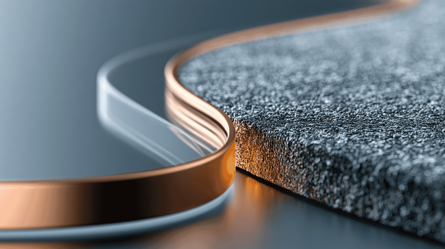
🔌 Everyone talks about the GPU at the heart of an AI server. Almost nobody asks what it sits on.
That base, the thin slab that carries a chip's wiring, is switching from silicon to glass. And the thing holding that switch back turned out to be almost comically basic: glass is too smooth for wires to stick to. At a trade show at Tokyo Big Sight in June 2026, Nikon, the company you know for cameras and microscopes, showed a way to beat that problem using light.
Why the floor under your chip is turning to glass
Modern AI chips aren't single slabs of silicon anymore. A high-end accelerator is really a cluster of smaller chips: a GPU here, stacks of high-bandwidth memory there, wired together inside one package. The piece that holds those chiplets and routes the thousands of connections between them is called an interposer, or substrate. Picture a tiny, ultra-dense motherboard sitting directly under the chip.
For years that layer was made of silicon or organic resin. But as AI packages grow larger and denser, those materials start to warp and lose signal quality. Glass is the industry's answer: it stays flat, holds its shape under heat, and loses less of a high-frequency signal on the way through. That's why nearly every major player (Japan's DNP, TOPPAN and Rapidus, Korea's SKC and Samsung, plus TSMC and Intel) is racing toward glass substrates, with volume production widely pegged to somewhere between 2027 and 2030.
There's just one inconvenient problem with glass.
The dilemma: glass is too smooth to wire
Glass is an insulator, so you can't simply electroplate copper wiring onto it the way you can on metal. And its mirror-smooth surface, the very thing that makes for clean signals, gives the wiring nothing to grip. Copper laid on flawless glass tends to peel.
The old fixes each came with a catch. You could roughen the glass by etching it, giving the copper texture to cling to, but a rough surface wrecks the very signal quality you switched to glass for. Here's why: at the high frequencies AI chips run at, current doesn't flow through the core of a wire, it skims along the surface, like a runner hugging the inside edge of a track. Make that surface bumpy and the signal takes a longer, rougher path, leaking energy as heat. The other option was to coat the glass inside a vacuum chamber by sputtering on metal. It works, but it needs expensive equipment.
So the industry was stuck choosing between smooth-but-won't-stick and rough-but-lossy.
Painting the grip with light
Nikon's answer, shown at JPCA Show 2026 on June 10 to 12, is a light-responsive surface material it calls PAP, short for Photo Assist Patterning. You coat the whole glass surface with it, then shine light only where you want wiring. The illuminated areas become able to hold a plating catalyst, so copper forms there and nowhere else.
The clever part is what it doesn't do. It never roughens the glass. The PAP film is under 10 nanometers thick, thin enough that the glass stays as smooth as before, so signal quality survives while the wiring still grips. The trade-off that had blocked glass for years simply dissolves. And because the process is a coat-and-expose step rather than a vacuum operation, it sidesteps the pricey chamber too. Glass is not the only target either: Nikon also has hard-to-plate organic substrates in mind.
Nikon says the material grew out of its work on organic materials for cameras and microscopes. Optical chemistry, repurposed. PAP was selected for the 22nd JPCA Award at the show. Tellingly, it wasn't the only glass-adhesion fix honored: Iox's plating-primer material for through-glass substrates took the same award at the same event, a sign of how hard the whole industry is pushing on this one bottleneck.
One caution worth keeping in mind: this is a technology demonstrated at a trade show, not yet a proven mass-production line. Nikon itself calls it a research-stage material and lists further work on the adhesion mechanism and reliability testing as what comes next. Glass substrates themselves are still a couple of years from volume. PAP is a strong answer to a real problem, not a finished revolution.
Who really owns the floor under the chip
Step back, and PAP fits a pattern that should make any country look hard at its supply chain. The flashy names in AI silicon are American and Taiwanese: Nvidia, TSMC. But the unglamorous materials that make those chips physically possible are heavily Japanese.
The clearest example is already inside almost every PC you've ever used. The insulating film that separates the wiring layers in high-end chip packages, called ABF, is made by Ajinomoto, yes, the seasoning company, which holds roughly 95% of that market, and close to 100% for PC processors. In package assembly, two Japanese firms, Ibiden and Shinko Electric, are said to hold 70 to 80% of the high-end share. In glass cores, DNP and TOPPAN are out front. Now Nikon is staking a claim on the surface chemistry that makes glass usable at all.
There's a comeback buried in that last one. Nikon once led the lithography machines that print chip circuits, then lost that front-end crown decisively to the Netherlands' ASML, which today owns the entire market for cutting-edge EUV machines. Rather than fight that battle again, Nikon and Canon have pivoted to the back end, the packaging side, where Nikon is now pushing both a large-panel exposure tool and materials like PAP. It's less a head-on rematch than an attempt to win from the side.
None of this shows up on a spec sheet, but the substrate has a supply chain, and that supply chain has chokepoints.
So here's the question. That AI server humming in a data center near you: the chip inside might be designed in California and printed in Taiwan. But the invisible slab it stands on? Look closely at who makes that, and ask whether, in your country, anyone does.





Global Discussion
0 comments