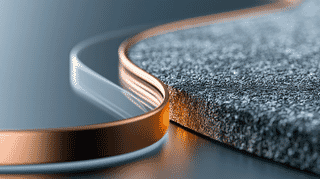
Glass is the front-runner for AI chip packaging substrates, but its smooth surface won't hold wiring. Nikon's new PAP material uses light to solve it. A look at the hidden Japanese chokepoints in the chip-substrate supply chain.
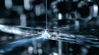
RIKEN and Enplas drill 1.1-micron, aspect-ratio-1,000 holes through glass in under a nanosecond, hitting 3,000 holes a second. As the chip race shifts from shrinking to packaging, here's why glass through-glass vias matter, and where Japan's materials and equipment makers fit.