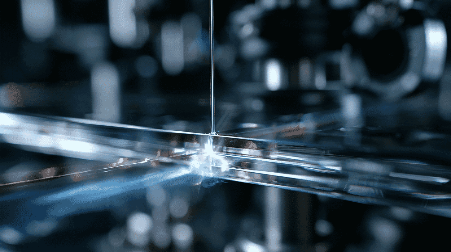
🔬 A hole thinner than a human hair, drilled a thousand times deeper than it is wide, punched clean through glass in less than a billionth of a second. The system already makes 3,000 of them every second. This is not a lab curiosity. It is a piece of the next semiconductor war, and it is being fought inside holes you will never see.
On June 10, 2026, Japan's national research institute RIKEN and Enplas Research announced what they call the world's fastest method for drilling tiny through-holes in glass. To most people that sounds like a footnote. To anyone tracking where chips are headed, it lands closer to the center of the board than the headline suggests.
The end of "just make it smaller"
For half a century, progress in chips meant one thing: shrink the transistors, pack more onto a single slab of silicon, repeat. That game is running out of room. The physics gets brutal and the cost of each new step gets absurd. So the industry has swapped the question. Instead of "how small can one chip be," it now asks "how well can we wire many chips together."
That shift has a name: chiplets and 3D packaging. Rather than one giant, perfect chip, you build several smaller specialized ones (logic here, memory there) and stitch them into a single package as if they were one. The high-end AI accelerators behind today's data centers already work this way. The foundation they all sit on is called an interposer.
For years interposers were made of silicon or organic resin. The next generation is expected to be glass. Glass is exceptionally flat and dimensionally stable, it warps little with heat, and it loses less energy at high frequencies, all the things you want when you are squeezing thousands of connections into a postage-stamp area. But to actually use a sheet of glass as wiring, you have to run electrical paths straight through it, top to bottom. Those vertical channels are called TGVs: through-glass vias. And drilling them turns out to be the hard part.
Drilling glass is harder than it sounds
Glass does not cooperate. It is brittle, so it cracks and chips. The holes have to be vanishingly thin yet deep. An aspect ratio of 1,000 means a channel a thousand times longer than it is wide, like a drinking straw stretched the length of a football field. The inside walls have to be smooth, or the metal plated into them later won't stick and the connection fails. And for a factory, none of it matters unless you can do it fast.
That last requirement is where existing methods stall. Conventional glass drilling tops out at a few hundred holes per second, and it often relies on a multi-step recipe: blast the glass with a laser to chemically alter a spot, then bathe it in a chemical etchant to dissolve the altered material, then clean, then repeat. It works, but it is slow, and slow is fatal when a single advanced package may need hundreds of thousands of holes.
Five laser pulses, one impossibly deep hole
The RIKEN-Enplas team took a different route. They used a laser running in what is called GHz burst mode: instead of firing one pulse, it fires a tight train of pulses spaced fractions of a nanosecond apart. Then they reshaped that beam with a cone-shaped axicon lens into a Bessel beam, a special form of light that, unlike an ordinary focused beam, does not spread out as it travels. It stays needle-thin all the way down.
The result: a single burst of just five pulses, fired once at a 1.1-millimeter sheet of borosilicate glass, bores a clean through-hole 1.1 micrometers wide, with no taper and no surrounding cracks. The laser is on for less than a nanosecond per hole, which the team clocks at more than 20,000 times faster than conventional drilling. A separate sodium-hydroxide bath afterward can widen the hole to any diameter you want, growing in proportion to soak time while keeping the channel uniform top to bottom. Measured wall roughness came in at 0.072 micrometers, mirror-smooth by the standards of this work. By moving the glass under the beam, the team has already reached 3,000 holes per second, and says a better motion stage should push past 10,000.

Source: RIKEN press release (June 10, 2026)
There is a small human story tucked into the official announcement. According to the press release, Enplas researcher Yuhei Miyahara says he approached RIKEN's laser group simply out of curiosity, wanting to try their GHz burst-mode technique on glass, and was welcomed in. The mode is notoriously fiddly: the number of possible settings explodes, and at first, he recalls, it was hard to tell what was even happening inside the glass. What turned it around was guidance on which parameters to chase first. The breakthrough, in other words, was less a single eureka than a borrowed tool pointed at a new problem by people who knew where to look.
Who's lining up for the next battlefield
To see why a drilling method matters, look at who else is at the table. The starting gun, by RIKEN's own account, was fired in September 2023, when Intel said it would bring glass-core substrates into mass production in the second half of the decade. In January 2026, at the NEPCON Japan show in Tokyo, Intel showed a working "thick-core" glass substrate paired with its EMIB packaging, and reports noted it avoided the micro-cracking that plagues brittle glass. Samsung Electro-Mechanics is aiming at mass production from 2027 onward, TSMC is developing its own glass-based panel packaging, and Japan's Rapidus showed a prototype large-format interposer built on a 600 mm-square glass carrier at SEMICON Japan in December 2025, with mass production targeted for 2028. South Korea's Absolics, an SKC subsidiary backed by an investment from Applied Materials, has already completed a dedicated glass-substrate plant in Covington, Georgia, at a cost of roughly $220 million.
Here is the part that is easy to miss. Most of those names are packaging houses and chipmakers that assemble the final product. But none of them can build a glass interposer without two things upstream: the glass itself, and a way to drill it cleanly and fast. That upstream layer is where Japan holds unusually strong cards. AGC and Nippon Electric Glass both make TGV-ready glass for advanced packaging; Nippon Electric Glass has paired with Via Mechanics, a leading drilling-equipment maker, to nail down the process. The RIKEN-Enplas laser slots into exactly this layer: not the headline contest over who ships the package, but the unglamorous contest over who supplies the materials and machines that make the package possible.
A caveat: this is a research result presented at a conference, not a production line. The leap from 3,000 holes a second in a lab to billions of flawless holes in a fab is real and unfinished. But the direction is unmistakable.
The contest has moved inside a hole you'll never see
For decades, the bragging rights in chips belonged to whoever could carve the smallest feature. That trophy still matters, but the action is sliding sideways: toward how chips are joined, what they sit on, and who can drill the cleanest path through a sheet of glass faster than anyone else. The phone or laptop you are reading this on is almost certainly held together by connections like these, and the ones a few years from now may run straight through glass. Where does your country sit in this quieter race: making the chips, packaging them, or supplying the tools that everyone else depends on?
References
- RIKEN press release (June 10, 2026): https://www.riken.jp/press/2026/20260610_1/index.html
- LPM 2026 (International Symposium on Laser Precision Microfabrication): https://www.clemson.edu/cecas/lpm2026/
- TrendForce, glass substrate landscape (May 2026): https://insights.trendforce.com/p/glass-substrate-development
- Nippon Electric Glass, large-format TGV glass-core substrate: https://www.neg.co.jp/news/20250522-1.html
- AGC, through-glass via products: https://www.agc.com/products/electoric/detail/tgv.html









Global Discussion
3 comments