
📷 The chip that turns light into the photo on your phone is very often a Sony part. On July 28 an earthquake stopped one of the plants that makes it. Two weeks later, Sony and TSMC signed a binding contract to put about 747 billion yen ($4.7 billion) into another one a few kilometres away. The contract contains something the world's largest contract chipmaker almost never agrees to: it is not the one in charge.
What the two companies actually signed
On August 11, 2026, Sony Semiconductor Solutions and TSMC announced a legally binding definitive agreement to create a joint venture, Advanced Vision Semiconductor Manufacturing Corporation, or AVSM, based in Koshi City in Kumamoto Prefecture. Its job is to develop and mass-produce smartphone image sensors using advanced process technology. As of the August 2026 announcement, volume production is planned to begin in 2029.
Sony contributes roughly 465 billion yen ($2.9 billion). Only part of that is cash. The rest comes from transferring a fab Sony has already built in Koshi into the new company through a corporate split. TSMC contributes about 282 billion yen ($1.8 billion), all of it cash. Kyodo News reported the resulting ownership as 62% Sony and 38% TSMC, which matches the ratio of the two contributions. Control sits with Sony alone, the venture goes onto Sony Group's consolidated accounts, and Sony appoints the representative director.
Both companies said the money will go in stages, keyed to market demand and business conditions. Filling the building with actual capacity depends on a further piece that is not yet settled: additional financing, which the two say they are pursuing on the assumption that the Japanese government will help.
Sony and TSMC signed a non-binding memorandum back in May. This is the version with legal teeth.
TSMC agreed to be the junior partner, and that is strange
TSMC's overseas ventures normally look nothing like this. In JASM, the company that runs TSMC's Kumamoto fabs, TSMC holds roughly 86.5%, with Sony at 6.0%, Denso 5.5% and Toyota 2.0%. In ESMC, the Dresden venture with Bosch, Infineon and NXP, TSMC holds 70% and the three European partners 10% each. In both, TSMC holds the majority and runs the fab.
In Koshi, TSMC holds 38% and does not pick the boss.
The inversion follows from what each side brings. Sony keeps core technology development, product planning and product design. TSMC supplies advanced process technology and manufacturing know-how, and the venture combines the two to get sensors into volume production faster.
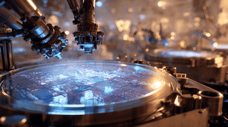
A modern phone sensor is not a single chip. It is at least two, bonded face to face: a top layer that catches light, and a logic layer underneath that reads the signal, converts it and increasingly interprets it before the phone's main processor ever sees it. The top layer is Sony's home turf. The bottom layer is an ordinary advanced logic chip, which is precisely what TSMC exists to make: in 2025 it ran 305 process technologies and produced 12,682 products for 534 customers, and as a pure-play foundry it builds them for clients rather than selling chips of its own. Neither company has said which process node the venture will use. Sony could have spent years and a fortune closing that gap alone. Instead it brought in a partner and kept control.
Why build here, two weeks after the ground moved
The 2026 Kumamoto Earthquake hit at 4:27 p.m. on July 28 with a magnitude of 7.1, registering the top level of 7 on Japan's shindo intensity scale in Uki City and Hikawa Town. In an advisory issued on August 10, the day before the contract was signed, Japan's meteorological agency was still warning that shaking of shindo 5-lower or stronger was likely in the worst-hit areas for about another month.
Sony's existing sensor plant, the Kumamoto Technology Center in Kikuyo, the town next door to Koshi, took shindo "upper 5" and shut down that afternoon. It restarted in phases from August 4, and at its quarterly earnings briefing on July 31 Sony said it expected the site back at pre-quake output by mid-August. When the same plant was hit in 2016, getting there took a little over three months. The difference is the decade in between: seismic reinforcement, restraints that stop equipment toppling, and continuity plans written in the aftermath of the last one.
So part of the answer to "why here" is that the last earthquake already happened and the buildings have been rebuilt around what it taught. The rest of the answer is the cluster. JASM's first fab in Kikuyo is in production, a second is under construction, and equipment and materials suppliers have followed them in. Wafers, engineers and spare parts move around Kumamoto in minutes rather than days.
The uncomfortable version of the same fact is that Sony is putting its newest sensor capacity a few kilometres from a plant that two major earthquakes have now stopped in the space of ten years. Recovering fast is not the same as not being exposed. Sony's implicit answer is that it would rather build where it already knows how hard the ground can shake.
From 180 billion yen to 747 billion yen in four months
In April, Japan's Ministry of Economy, Trade and Industry certified a supply plan for the Koshi fab under the country's economic security law: 180 billion yen ($1.1 billion) of total investment, capacity of 10,000 wafers a month in 300mm equivalent, supply starting May 2029, and a subsidy of up to 60 billion yen ($380 million).
Four months later, the same site anchors a 747 billion yen joint venture.
The two figures are not measuring the same thing. Sony's contribution includes handing over a building it had already paid for, so this is not 747 billion yen of fresh construction. But the direction is hard to miss. As sensors take on more logic, the plant that makes them stops resembling a specialty fab and starts resembling a leading-edge logic fab, and leading-edge logic fabs cost leading-edge money. A camera component has become an expensive computing component.
Three ways to organise a chip industry, and a fourth
Advanced chip manufacturing is usually organised in one of three ways.
Taiwan runs the pure-play foundry model TSMC invented in 1987: the foundry owns and runs the fabs, and its customers buy capacity instead of building it. The United States pays foreign firms to build fabs on American soil that those firms own outright. China channels state money into vertical self-sufficiency, aiming to control every step from design through materials.
Koshi is a fourth shape. The customer owns the fab. The foundry contributes process knowledge and takes equity instead of control. Japan gets the plant and the jobs, Sony keeps the design crown jewels, and TSMC earns returns from a product it does not sell in competition with Sony.
Whether that shape travels anywhere else is an open question. It works here because Sony is a rare customer that already knows how to run fabs, and because the thing that makes the product special belongs to the customer rather than the foundry.
What still has to go right
Closing depends on regulatory approvals and the usual conditions. The funding is staged against demand, so a soft smartphone market would slow it. The capacity plan leans on government support that has not been finalised. And volume production is still three years away.
Against all that, what both sides are buying is a share of the eyes of the world's phones.
In Japan, part of that bill is public. Where you live, would your government be helping to pay for a factory like this, and would you want it to?
References
- https://www.sony-semicon.com/en/news/2026/2026081101.html
- https://japantoday.com/category/tech/update2-sony-semiconductor-tsmc-to-invest-747-billion-yen-in-next-gen-sensors
- https://www.sony-semicon.com/ja/info/2026/2026073101.html
- https://www.itmedia.co.jp/news/article/2607/31/2000000341/
- https://kumanichi.com/articles/2021449
- https://www.jma.go.jp/jma/menu/20260728_kumamoto_jishin.html
- https://www.meti.go.jp/speeches/kaiken/2026/20260417001.html
- https://eetimes.itmedia.co.jp/ee/articles/2604/17/news121.html
- https://www.sony-semicon.com/en/news/2024/2024020601.html
- https://www.infineon.com/press-release/2023/infxxx202308-144







Global Discussion
3 comments