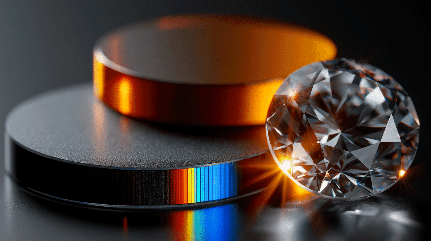
💎 The most famous name in diamonds just teamed up with a small factory in northeast Tokyo, and together they grew one of the largest single-crystal diamond wafers ever made: three inches across. This is not a jewelry story. Diamond is what many engineers call the ultimate semiconductor, and whoever can grow it big enough to mass-produce will help decide what comes after silicon carbide.
From watch jewels to semiconductor wafers
Orbray is not a household name, even in Japan. The company started in 1939 as Namiki Manufacturing, making the tiny sapphire bearings that kept electric meters running. Over the decades it moved into phonograph needles, watch jewels, magnetic heads, and the miniature vibration motors inside pagers and early mobile phones, a market it once largely owned. The thread running through all of it was never a single product. It was a skill: cutting, grinding, and polishing the hardest materials on Earth to nanometer precision.
That skill carried a maker of jewel bearings to the edge of the semiconductor industry. Based in Tokyo's Adachi ward and led by president Riyako Namiki, Orbray grows and shapes sapphire, ruby, and diamond for everything from fiber optics to medical instruments. Diamond is the one power-electronics engineers have been chasing for years.
The reason is physics. Diamond has the widest bandgap of any practical semiconductor, around 5.5 electron-volts, versus 3.3 for silicon carbide and 3.4 for gallium nitride. It also conducts heat better than any other bulk material known, above 2,000 watts per meter-kelvin, roughly five times silicon carbide and ten to twenty times gallium nitride. In plain terms, that means chips that can run hotter, switch faster, and handle far higher voltages in a smaller space. The catch was always the same: nobody could make diamond big.
Why you can't just grow a bigger diamond
The cleanest way to grow a single crystal of diamond is on top of another diamond, a method called homoepitaxy. But you have to start somewhere, and large, high-quality diamonds do not exist in nature to seed the process. Worse, the technique can't produce a crystal wider than the seed beneath it. So the size of your starting diamond caps the size of everything you make.
The way around this is to grow diamond on a different, larger material, such as sapphire. This is heteroepitaxy, and in theory a big sapphire wafer should yield an equally big diamond. In reality the two materials fight. As the diamond layer forms, the mismatch with the sapphire underneath builds up enormous internal stress, and the crystal cracks apart. Salvaging any usable area meant fabricating fragile microneedle structures to relieve that stress, an extra step that was hard to manufacture and costly. The larger the target, the worse the cracking. That one problem, stress, is what kept device-grade single-crystal diamond stuck at sizes measured in millimeters while silicon marched on to 300.
A tilt in the sapphire
Orbray's way out came from the part of its business that looked least strategic: sapphire. It is one of the few companies that can grow very large sapphire crystals, and it learned to control their orientation with great precision. By growing diamond on a sapphire surface cut at a deliberate angle, the company developed what it calls step-flow growth, in which the crystal builds outward in orderly lateral steps, like a staircase. The stress now travels sideways through the layer instead of building to the breaking point, so the microneedles became unnecessary.
That approach produced a two-inch heteroepitaxial diamond in September 2021, a size the field had treated as a benchmark. But going from one good two-inch crystal to a reproducible, manufacturable process at larger diameters is a different kind of challenge, one about yield, uniformity, and volume rather than a single lucky result. For that, Orbray needed a partner with deep pockets and deep diamond knowledge. In June 2024 it found one in an unexpected place.
The diamond giant and the Tokyo workshop
Element Six is the synthetic-diamond arm of De Beers, the company most of the world ties to engagement rings. De Beers has been in the industrial-diamond business since the 1940s, and Element Six, headquartered in London, has spent decades turning lab-grown diamond into things other than gemstones. Its diamonds sat inside the CERN detectors that helped confirm the Higgs boson. The US defense research agency DARPA chose the firm to develop large, device-quality diamond substrates for military electronics. When a company like that goes hunting for a partner to scale up single-crystal diamond, it says something about where the technology is going.
On paper the match was clean. Orbray had the sapphire-based growth method; Element Six had large-area deposition systems, high-purity diamond expertise, and a chemical-vapor-deposition plant in Gresham, Oregon. On June 16, 2026, the two announced their first joint result: a reproducible process for three-inch single-crystal diamond wafers, 76.2 millimeters across. Forget the headline number for a second, because the word that matters is reproducible. A one-off crystal is a lab demo. A repeatable process is the beginning of a supply chain.
The roadmap is specific. Two-inch wafers for heat-management uses are heading into volume production at the Oregon plant from July 2027, with a second two-inch product tuned for building devices close behind. Three-inch volume production is targeted for 2028 and beyond. Development of four-inch wafers, the size that fits straight into existing semiconductor lines, has already started, with mass production aimed at 2030 onward.
What a blank wafer decides
The timeline deserves some honesty. Diamond power devices are not expected to ship in volume until the end of this decade at the earliest. Diamond is punishing to process precisely because it is the hardest material there is, and getting its electrical behavior under control remains difficult. Even a four-inch wafer is tiny next to silicon's 300-millimeter wafers and silicon carbide's 200-millimeter wafers. One announcement does not erase any of that.
But the real bottleneck in diamond electronics was never the devices. It was the substrate, the blank wafer everything else is built on. Without a steady supply of large, uniform single-crystal diamond, none of the promised uses (6G wireless, high-power and radio-frequency electronics, sensors, heat spreaders, quantum hardware) can leave the lab. That is the exact piece Orbray and Element Six are now trying to industrialize, and it is why a Tokyo workshop's sapphire trick suddenly matters to a British mining conglomerate and to American defense planners. The two-inch volume production will run on US soil, in Oregon, right alongside Japanese growth technology. The next material era is being assembled across borders, not inside any one of them.
Japan has held an unusually strong hand in diamond substrates for years, from Orbray's wafers to the university labs and startups building the devices that sit on top of them. (kantenna has covered the device side, including a world-first diamond MOSFET switching demonstration, as well as Orbray's separate (111) substrate aimed at quantum sensors.) The workshop that once made the buzzing motor in your old pager is now helping decide what will power the data centers and 6G base stations of the 2030s.
In your country, is diamond talked about as a future chip material, or still mainly as something that goes in a ring?
References
- https://newswitch.jp/p/49487
- https://www.semiconductor-today.com/news_items/2026/jun/elementsix-orbray-160626.shtml
- https://www.debeersgroup.com/our-business/synthetics-diamonds
- https://orbray.com/
- https://kantenna.com/topic/diamond-mosfet-world-first-200v-1a-switching-power-semiconductor
- https://kantenna.com/topic/diamond-mosfet-dc-dc-converter-world-first-power-conversion






Global Discussion
0 comments