🔬 Whatever screen you are reading this on, the molecules producing the light are not lined up.
Organic films laid down by vacuum evaporation freeze in place with their molecules pointing every which way. That has been the standard for OLEDs since the beginning. A group at the University of Toyama has now turned that layer into a crystal without giving up the practical thin-film stack around it. At the same 1 volt, current ran up to 1,000 times harder.
Piling molecules up in a mess became the standard
Phone screens and television panels are built much the same way. Organic materials are evaporated in a vacuum chamber and allowed to settle onto a glass or plastic substrate. Stack every layer together and you still only get a few hundred nanometers of thickness. The process is fast, reliable, and scales to large areas.
What it does not do is arrange anything. The molecules land in whatever orientation they happen to land in and stay there. This is what amorphous means: no crystal order. Because neighboring molecules barely overlap, electrical charge struggles to hop from one to the next, and the film never delivers what the material itself is capable of.
This is where OLED history starts. In 1987, Ching W. Tang and Steven A. VanSlyke at Eastman Kodak ran current through two thin organic layers and got green light out of them. That device was the template, and for nearly four decades the industry has pushed efficiency and lifetime forward inside the same framework of stacked amorphous films.
Everyone already knew crystals were better
Line the molecules up into a crystal and charge moves far more easily. Organic single crystals have attracted attention for exactly that reason.
The obstacle was never the idea. It was installation. The usual way to grow a good crystal film is epitaxy, where the film takes its ordering cue from the crystal lattice of the substrate underneath. Epitaxy needs a special substrate, and slipping that requirement into a device made of many stacked thin films is close to impossible. Good crystals and working devices were each achievable; nobody could get them in the same object.
Rubrene, the organic semiconductor at the center of this work, embodies the problem. As a single crystal it has one of the highest charge mobilities of any organic material. Evaporate it into a thin film the normal way and it comes out amorphous.
Seed it, build the device, then let it grow
The University of Toyama announced the work on July 27, 2026. Professor Masahiro Morimoto of the Academic Assembly Faculty of Engineering, working with Yuya Honda and Professor Shigeki Naka, solved it by reversing the order of operations.
They started with a glass substrate carrying an indium tin oxide electrode and laid down an underlayer of α-NPD, an amorphous material with a low glass-transition temperature. Low glass-transition temperature means its molecules start moving at relatively modest heat. On top went 50 nanometers of rubrene.
Heat comes next. The first round leaves crystal seeds scattered through the rubrene, too small to see. Rather than grow them there, the team finished building the device on top of them and heated it again. The second round softens the underlayer, and the seeds widen into the room that new mobility opens up.
The point of this two-step annealing is the sequencing. The crystal is not made and then built into a device; the device is built and then the crystal is grown inside it. No special substrate is involved anywhere, which is why the university describes the result as a non-epitaxial crystalline thin film.
A one-millimeter crystal inside a 50-nanometer film
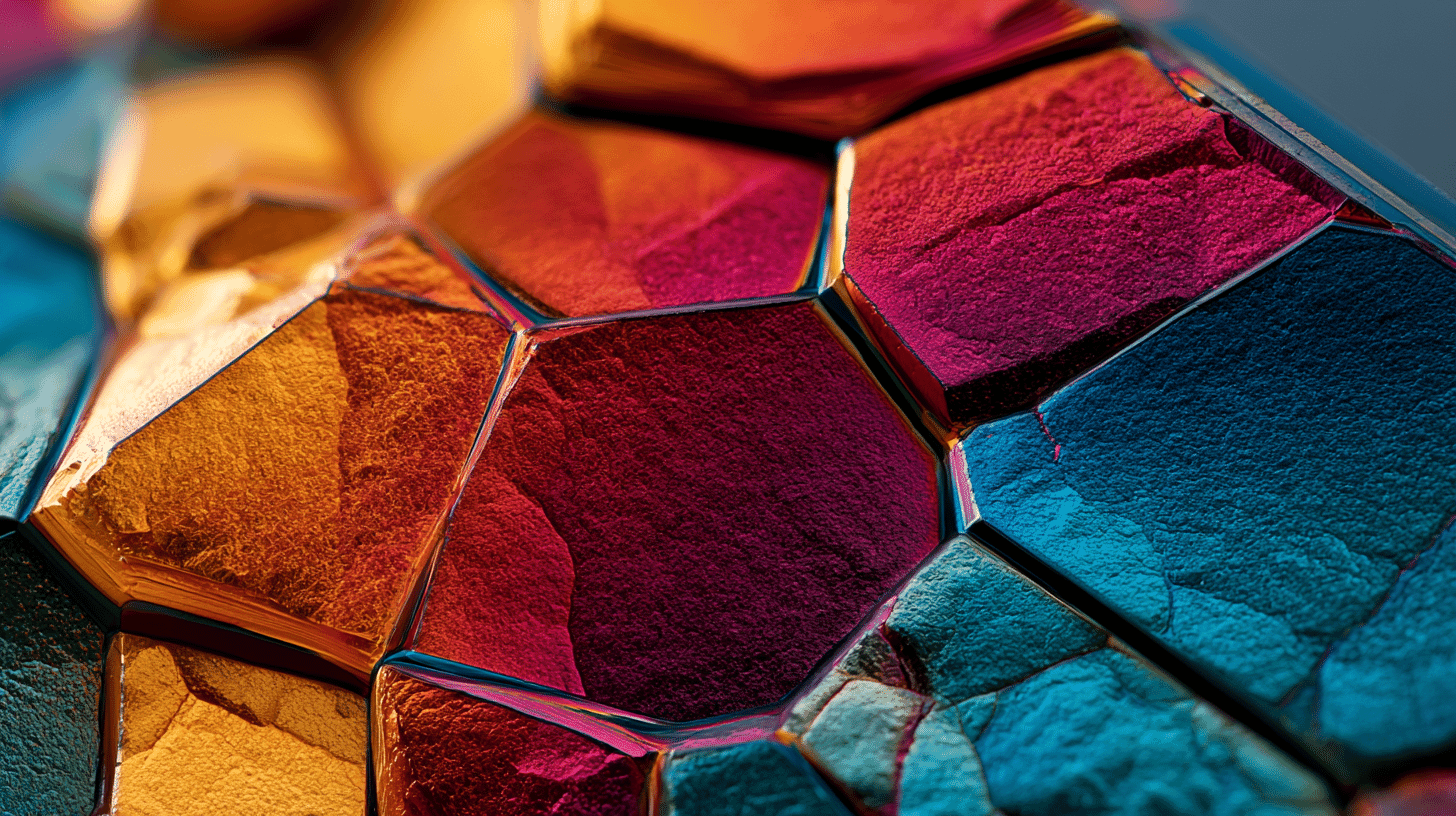
What that produced shows up under a polarizing microscope as crystalline domains around 1 millimeter across, and not in one lucky spot: the same pattern repeats over the whole 25-millimeter substrate, so growth was even rather than patchy. X-ray diffraction pinned the structure down as orthorhombic.
The film is 50 nanometers thick. The crystal is 1 millimeter wide. That is twenty thousand to one. A layer no thicker than the skin of a soap bubble holds a patch of single crystal big enough to see without a microscope.
How to read 1,000-fold and 1.33 volts
Hold the voltage at 1 volt and the crystalline device pushes up to 1,000 times the current density of its amorphous twin. It also starts glowing sooner: current begins to flow at 0.38 volts, and luminance reaches 1 cd/m² at 1.33 volts, a drop of 0.30 volts.
The light itself came out different. Where amorphous rubrene spreads its emission across two wide humps, the crystalline device concentrated it into one narrow line at roughly 565 nanometers. The university attributes that to a single transition dipole moment, which is another way of saying the molecules now point the same way. In a display, narrower emission means purer color and a wider gamut.
Nobody invented a new emitter here. The material is the same rubrene it always was; only its arrangement changed. So the 1,000-fold figure is best read as performance the amorphous film had been sitting on, finally getting through. In the university's English release, Morimoto says the work "represents the first application of non-epitaxial crystalline thin films to OLEDs."
Brighter, and less efficient
It is not all upside. The release lists emission conversion efficiency as an open problem, because it drops in relative terms once the layer crystallizes. Charge moves easily now; turning that charge into photons is where the crystalline device still loses to the amorphous one. The group plans to address this with dopants chosen so they do not disturb crystallization.
Some things go unmentioned. Lifetime, a perennial sticking point in OLED commercialization, does not appear in the release at all. Neither does scaling to large areas or fitting a mass-production line. This is a single substrate in a laboratory, not a fab.
The release hedges what comes next, and reasonably so. If the technique matures, it says, the payoff could reach past more efficient, longer-lived phones and televisions to ultra-high-brightness displays, AR and VR devices, and organic semiconductor lasers, which need high current drive. Those are hopes, not schedules.
The paper appears in Volume 320 of the journal Synthetic Metals. It went online on July 1, 2026, with print publication dated August 1, 2026.
Where is the factory that would want this?
Suppose the method gets refined. Who turns it into a product?
As of July 2026, OLED panel manufacturing sits outside Japan. UBI Research put Samsung Display at 44.4 percent of the smartphone OLED panel market in the first quarter of 2026, with BOE at 16.3 percent and LG Display at 9.0 percent. Japan's own contender, JOLED, was formed in 2015 by merging the OLED divisions of Sony and Panasonic. In 2017 it became the first company to commercialize printed OLED panels. It filed for civil rehabilitation in March 2023 and withdrew from manufacturing and sales.
Against that, one detail is easy to overlook. This process asks for no exotic equipment: vacuum evaporation, which OLED lines already run, plus heat. There is no special substrate to source, as epitaxy would require. It is the kind of technique an existing factory could absorb.
In the university's English release, Morimoto frames OLEDs as standing at the same kind of turning point the semiconductor industry passed through once it learned to control structural order precisely. For now, though, the only building where anyone can check is a university lab.
The screen in your pocket is still a jumble of molecules. How much attention does university research like this get where you live, and what does the road from a lab bench to a factory floor actually look like there?





Global Discussion
3 comments