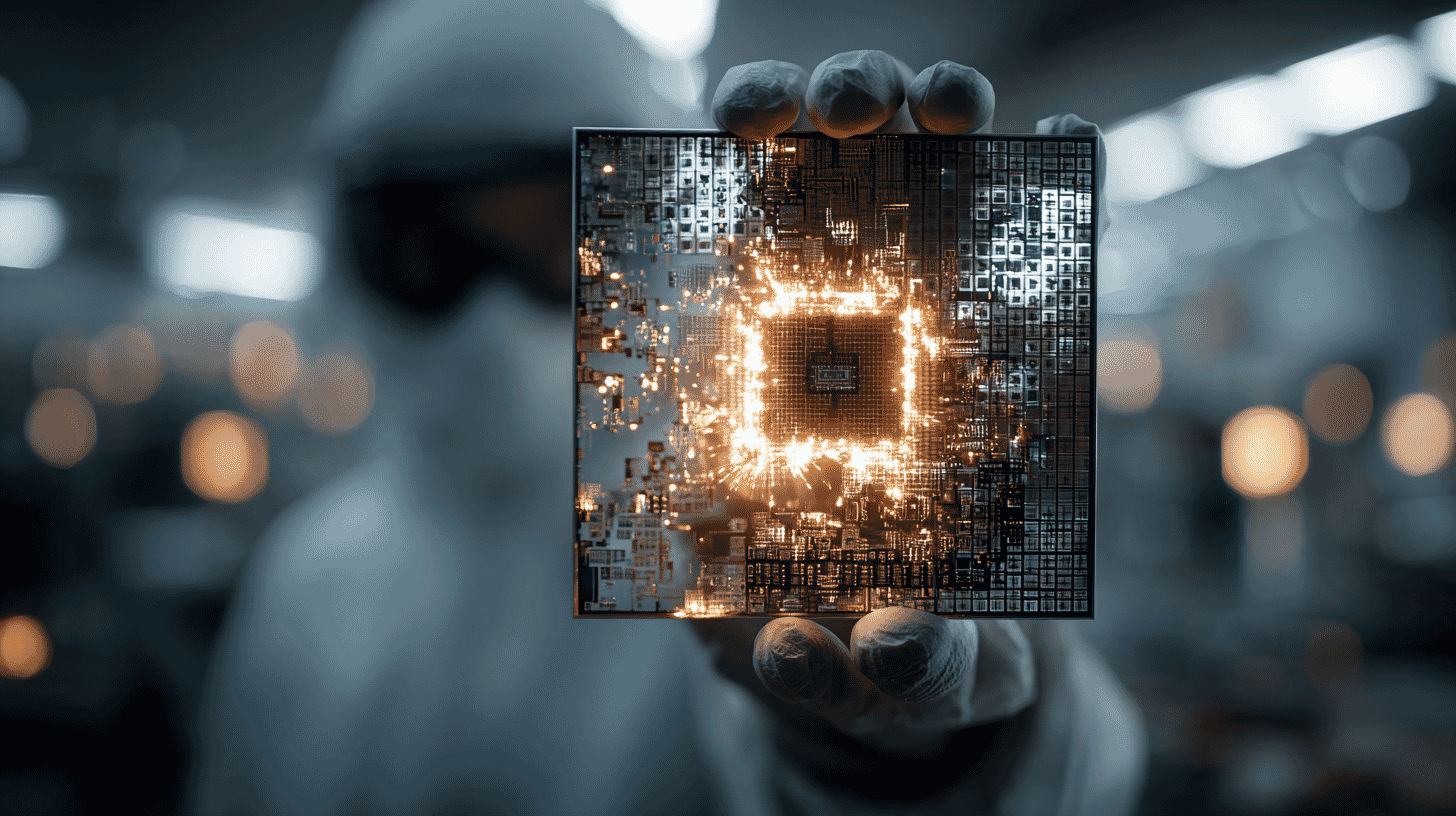
The future of semiconductors is shifting from circles to squares. Rapidus CEO Atsuyoshi Koike took the stage holding aloft the world's first 600mm square glass substrate. The technology raises production efficiency tenfold over conventional round wafers and could cut the manufacturing cost of AI chips. Into the contested world of advanced packaging, where TSMC and Intel battle, Japan has made its move. Here is what it amounts to, and what its chances are.
A World-First Substrate Unveiled at SEMICON Japan
From December 17 to 19, 2025, the international semiconductor exhibition "SEMICON Japan 2025" was held at Tokyo Big Sight. Before a packed hall, Rapidus CEO Atsuyoshi Koike took the stage and held up a huge panel with both hands. On the gold-gleaming panel, the number "600" was rendered in actual chips.
"This is what I wanted to show you," Koike said, unveiling a prototype of the world's first 600mm square RDL interposer (an intermediate substrate with a redistribution layer). Referring to how NVIDIA CEO Jensen Huang presents products by holding them up, Koike drew laughter by saying he had done 100 push-ups a day just to hold this panel, yet his expression was entirely earnest.
The prototype had just been completed at "Rapidus Chiplet Solutions" (RCS), a back-end research-and-development base being set up within Seiko Epson's Chitose site in Chitose, Hokkaido. Koike stressed that "there is no other example in the world of mass-producing front-end and back-end processes in the same factory," showing that the core of Rapidus's differentiation strategy lies in this technology.
Why a "Square Substrate" Is Revolutionary
For readers unfamiliar with semiconductors, let's cover the basics.
Current semiconductor manufacturing standardly uses round silicon wafers 300mm (about 30cm) in diameter. Chips are formed on the wafer and then cut out. But because chips are square, the edges of a round wafer inevitably leave unusable space, so-called "edge loss."
Rapidus's 600mm square substrate overturns this convention. A square panel can be used right to the edge with no waste. Even a simple area comparison shows that against a 300mm wafer's area (about 70,700mm²), a 600mm square panel (360,000mm²) is more than five times larger. And because edge loss almost disappears, the yield per substrate jumps. A conventional wafer produced about four interposers; a single panel produces roughly 40, a tenfold gain.
There is an important point, though. This 600mm square substrate is not for making the chips themselves. It is the substrate for "placing and connecting" chips, that is, the intermediate substrate for packaging (the interposer).
What Is an Interposer? The "Wiring Board" of the AI Era
Today's high-performance AI chips are increasingly built not from one giant chip but by combining multiple small chips (chiplets). Compute chips such as GPUs and CPUs must be brought together in a single package with fast memory called HBM (high-bandwidth memory).
The interposer is the "foundation" that physically holds these chiplets and connects them with fine wiring. Thousands of wires run through it so the chips can communicate at high speed, making it a crucial component that determines a semiconductor package's performance.
The fact that AI chips grow larger with each generation also raises the interposer's importance. As Koike noted, "devices are getting bigger and bigger," and with NVIDIA's latest GPUs and the like, the total package area keeps expanding. Rapidus's interposer secures 1.3 to 2 times the wiring area of competitors, a design that can handle the next generation of ultra-large AI chips.
Rapidus's Secret Weapon: Repurposing LCD Panel Technology
Behind Rapidus's ability to achieve the huge 600mm size is an unexpected application of technology: the panel-handling techniques of the LCD display industry.
For the semiconductor industry, 600mm is an unknown, huge size, but for the LCD panel industry it is a "familiar size," even a small one. TV panel manufacturing has routinely handled giant glass substrates exceeding Generation 8 (2,200mm × 2,500mm). Rapidus brought this cross-industry expertise into semiconductor packaging.
The setup of RCS was led by Yasumitsu Orii (now a Rapidus senior executive officer), who had served as head of a former Sharp subsidiary. Orii also has a background handling packaging technology at IBM Japan, and is versed in both semiconductor micro-fabrication and large-area LCD panel handling. That cross-industry combination is what lets Rapidus pick a different battlefield from TSMC or Intel.
Comparing the Competition: TSMC's CoWoS, Intel's Foveros
TSMC's CoWoS (Chip-on-Wafer-on-Substrate) is the de facto standard for current advanced packaging. Most of NVIDIA's AI GPUs are made with it, and TSMC plans to expand from about 75,000 wafers per month at the end of 2025 to 120,000 to 130,000 per month by the end of 2026. Even so, demand is so strong that NVIDIA alone holds about 60% of capacity, forcing other customers into long queues. Because CoWoS is based on 300mm silicon wafers, it faces reticle (exposure-area) limits, and handling ultra-large packages requires "stitching" chips together.
Intel's Foveros is a 3D packaging technology that stacks chips vertically. It has high design compatibility with CoWoS and is drawing attention as an alternative to make up for TSMC's supply shortfall. Intel is expanding Foveros production capacity by 30% and EMIB (Embedded Multi-die Interconnect Bridge) by 150% at its New Mexico plant, and Apple, Qualcomm, and Broadcom are said to be evaluating the technology.
Samsung's I-Cube is a 2.5D packaging technology similar to TSMC's CoWoS, characterized by a design that leverages Samsung's strength as an HBM supplier.
TSMC itself is also developing a next-generation square-panel technology, CoPoS (Chip-on-Panel-on-Substrate). The direction Rapidus has chosen is not an industry outlier but one of the mainstream bets.
Against these, Rapidus's approach is fundamentally different. It uses square panels rather than round wafers, a "panel-level packaging (PLP)" approach, and the material is glass rather than silicon. Glass substrate is cheaper than silicon, has a low coefficient of thermal expansion (less distortion from temperature change), and offers lower loss of high-frequency signals.
The Strategy of Integrated "Front-End Plus Back-End" Production
Another key differentiator for Rapidus is the concept of carrying out the front-end (creating the chip's circuits) and the back-end (assembling chips into packages) integrated in the same factory. Koike stresses that "this is a world first."
Traditionally, semiconductor front-end and back-end processes have generally been done at different companies, and in different countries. Typically, chips are made at TSMC and then packaged at an OSAT (outsourced assembly and test company) such as ASE or Amkor, a division of labor that is the norm.
Rapidus makes 2nm chips at its IIM-1 plant in Chitose, Hokkaido, and completes packaging at the adjacent RCS. Under the "RUMS (Rapid and Unified Manufacturing Service)" model it advocates, it manages everything from design support through front-end and back-end in an integrated way, aiming to shorten the conventional semiconductor manufacturing cycle by 60%. In fact, it completed a 2nm prototype chip, which normally takes six months, in 12 days and 18 hours, a sign of its confidence in speed.
The Roadmap: Aiming to Start Mass Production in 2028
Rapidus plans to start mass production of back-end (packaging) in 2028. The front-end will begin mass production in the second half of fiscal 2027 at 6,000 wafers per month, expanding to 25,000 per month in fiscal 2028.
The plan called for standing up the RCS pilot line by March 2026 and beginning full-fledged research and development from April.
Update: the RCS back-end pilot line started operating in April 2026. Government backing was topped up as well: METI added ¥631.5 billion in R&D support in April, bringing cumulative R&D support to ¥2.354 trillion, and in June it completed a further ¥150 billion equity injection through the Information-technology Promotion Agency, taking the government's share of paid-in capital to roughly 60%.
On the business side, it aims to turn operating cash flow positive in fiscal 2029 and to list its shares in fiscal 2031. Government support is planned to total about ¥2.9 trillion (roughly $19 billion) through fiscal 2027, and whether Rapidus can deliver a return to match that is the open question.
Challenges and Prospects: Can It Carry NVIDIA's Chips?
The technical potential has been shown, but there are many challenges.
First, there is a large gap between prototype and mass production. Whether stable yield (the rate of good product) can be secured on a huge 600mm square panel is unknown. Panel-level packaging is still a developing technology across the industry, and many technical hurdles remain to stabilize quality in mass production.
Next is winning customers. Koike repeatedly referred to NVIDIA's CEO Huang and expressed his eagerness for contract manufacturing, saying he "sincerely hopes to place NVIDIA's chips" on the panel. But NVIDIA has built a firm partnership with TSMC, and it will not be easy for Rapidus to break in.
On the other hand, the fact that TSMC's CoWoS supply is stretched is also an opportunity for Rapidus. With the rapid growth of the AI chip market making "packaging the bottleneck of semiconductor supply," there is room for new players to enter.
Koike closed his talk with a vision video of a "2039 semiconductor factory": a fully automated, unmanned line on the first floor, humans and humanoid robots jointly managing production on the second. The room to talk about a future 14 years out is the flip side of confidence in the work at hand.
Japan's semiconductor industry held a 50% global share in the 1980s and lost its position over the following three decades. What Rapidus is betting on is not the chip itself but how chips are mounted. Whether that bet pays off turns on something far less cinematic: whether yields hold steady across a 600mm square panel.
In your country, what is the debate around government investment in the semiconductor industry and innovation in packaging technology? We'd love to hear about it.
References
- https://www.nikkei.com/article/DGXZQOUC191OL0Z11C25A2000000/
- https://www.nikkei.com/article/DGXZQOUC0944C0Z01C25A2000000/
- https://news.mynavi.jp/techplus/article/20251224-3865433/
- https://xenospectrum.com/rapidus-glass-substrate-plp-tsmc-rival/
- https://news.yahoo.co.jp/articles/0a37ce0e225072f144625c164bb2ca40cf879f0f








Global Discussion
15 comments