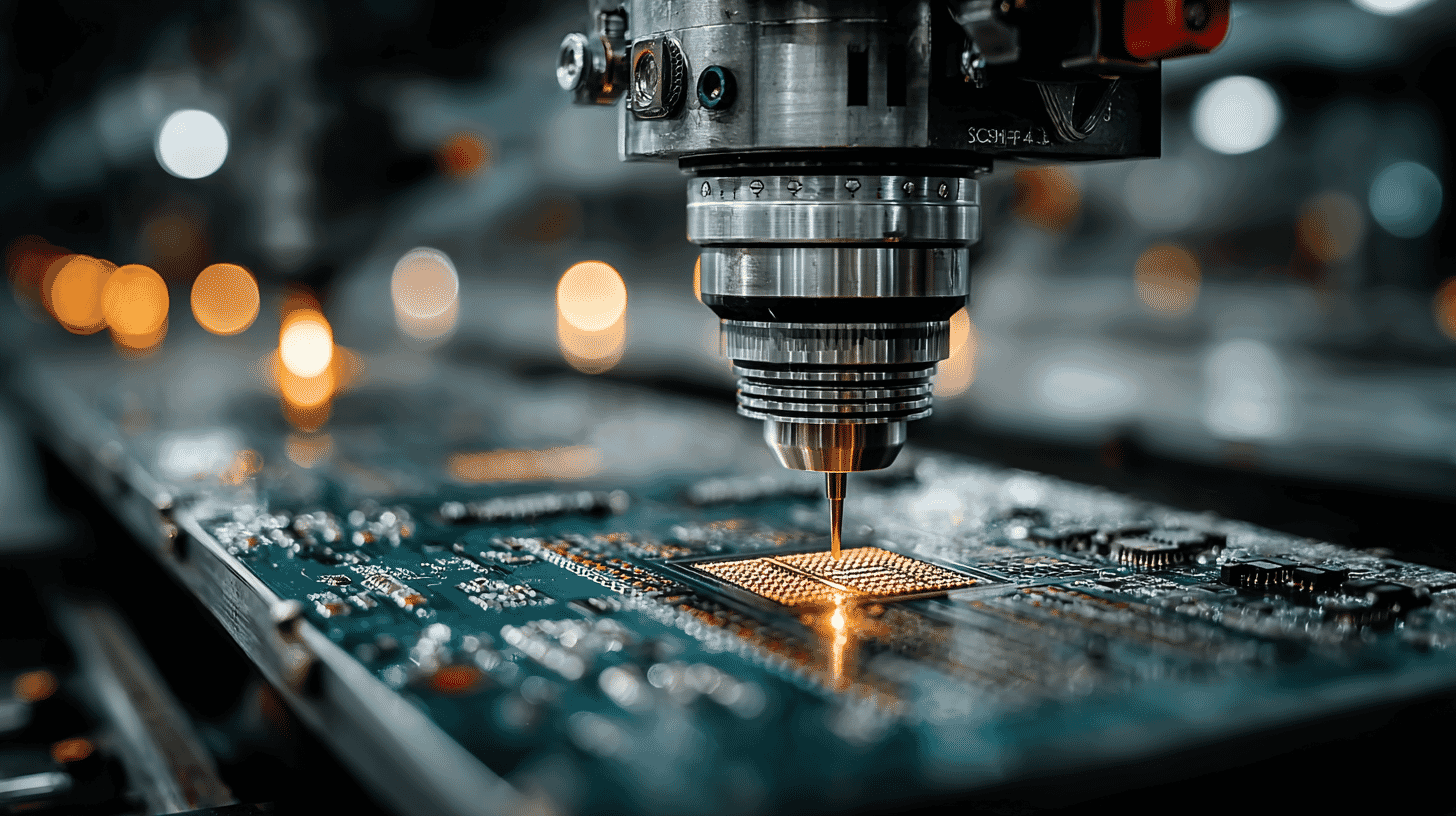
🔬 The machines that print the world's tiniest circuits are controlled by one company: ASML of the Netherlands. But Japan's Canon is fighting back with a bold strategy. Instead of chasing ASML's $350 million EUV machines, Canon is targeting the workhorses of chip factories: the KrF lithography tools used in dozens of layers that even the most advanced chips can't be made without.
With a global NAND flash shortage creating urgency and a $330 million factory expansion underway, here is how Canon plans to reclaim ground in the semiconductor equipment wars.
Canon Launches Its First New KrF Machine in 14 Years
In early 2026, Canon is rolling out a completely redesigned KrF (krypton fluoride) lithography system, its first new model in this category since 2012. While the company has steadily improved the previous generation's throughput to 310 wafers per hour over the years, the new machine represents a full architectural refresh, pushing processing speed to 400 wafers per hour, a 30% jump.
KrF lithography uses a 248-nanometer laser to pattern circuit layers with relatively larger feature sizes. While cutting-edge EUV (extreme ultraviolet) systems get most of the headlines, the reality of chipmaking is more nuanced. In a state-of-the-art fab producing advanced logic chips, there may be over 50 lithography steps, but EUV handles only 2–3 of them. The vast majority of layers rely on KrF, i-line, and other "mature" tools. Without them, even the most advanced chips simply cannot be manufactured.
Canon currently holds about 30% of the KrF lithography market by unit volume, and its target with the new machine is ambitious: capture over 50% market share. The primary customers are mega-fabs, factories processing over 100,000 wafers per month, run by the world's largest memory and logic chipmakers.
Why Now? The Global NAND Flash Crisis
The timing of Canon's KrF offensive is no coincidence. The world is in the grip of a severe NAND flash memory shortage that industry analysts are calling a "supercycle."
TrendForce initially projected NAND flash contract prices would climb 33–38% quarter-on-quarter in Q1 2026, then revised that to 55–60% in February. Phison's CEO has gone so far as to warn that the shortage could force many consumer electronics companies to shut down or exit product lines in the second half of 2026. IDC calls this not a typical cyclical downturn but a "potentially permanent, strategic reallocation of the world's silicon wafer capacity."
The root cause is AI. Hyperscalers like Microsoft, Google, Meta, and Amazon are consuming enormous quantities of HBM (High Bandwidth Memory) and server DRAM for AI infrastructure. The three largest memory manufacturers, Samsung, SK Hynix, and Micron, have responded by shifting their limited cleanroom capacity toward these higher-margin products. Every wafer allocated to an HBM stack for an Nvidia GPU is a wafer denied to the SSD in your laptop or the storage in your smartphone.
Compounding the issue, a severe HDD (hard disk drive) shortage is pushing data centers to substitute high-capacity enterprise SSDs, tightening NAND supply further. Industry estimates put 2026 NAND demand growth at 20–22% year-on-year, ahead of what suppliers plan to add.
Update, July 2026: NAND contract prices rose another 70–75% quarter-on-quarter in Q2 2026, outpacing DRAM for the first time in this cycle. TrendForce now forecasts a 10–15% increase for Q3, a slower climb but still no easing of the underlying shortage.
Canon's Seiya Miura, Executive Officer and head of the Semiconductor Equipment Division, frames the opportunity clearly: generative AI has been driving demand for logic chips and HBM, but now NAND is feeling the squeeze too. Memory makers prioritize productivity above almost everything else, and that's exactly what Canon's faster KrF machine delivers.
ASML's Dominance: Understanding the Landscape
Until the 2000s, Canon and Nikon together controlled over 70% of the lithography market. But when ASML successfully commercialized EUV lithography in the 2010s, the balance of power shifted dramatically. EUV systems use 13.5-nanometer wavelength light to pattern features at 5nm and below. Each machine costs roughly $200–300 million, and the latest High-NA EUV system approaches $350 million.
Today, ASML commands approximately 80–90% of the lithography market by revenue and has a complete monopoly on EUV. Canon and Nikon share the remaining slice.
However, the picture changes when measured by unit volume. Canon shipped 233 lithography systems in 2024, about 30% of the roughly 600 units sold industry-wide, making it the number-two player by volume. In i-line lithography, Canon holds a commanding 80% share. The company's 2025 target is 255 units, with growth expected to continue.
The revenue gap exists because a single EUV machine generates as much revenue as dozens of KrF or i-line systems. But volume matters too: fabs need these workhorse tools in large quantities, and reliable supply of high-throughput systems is a genuine competitive advantage.
Canon's Three-Pronged Strategy: KrF, ArF, and Nanoimprint
Canon's ambitions extend well beyond KrF.
ArF dry re-entry. Canon previously entered and then exited the ArF dry lithography market. In early 2026, the company is re-entering with a new, more competitive model. ArF dry systems use a 193nm laser and can pattern finer features than KrF, targeting semi-advanced power semiconductors. "It's not a huge market, but customers told us they wanted Canon to offer ArF," Miura explains, a clear signal of Canon's shift from technology-driven to customer-driven development.
Nanoimprint lithography (NIL). Canon's most radical bet is its FPA-1200NZ2C nanoimprint system, commercially launched in October 2023 as the world's first NIL tool for semiconductor manufacturing. Instead of using light to project circuit patterns, NIL physically stamps a template into resin on the wafer surface, like pressing a seal into wax.
The advantages are compelling: up to 90% lower power consumption compared to EUV, significantly lower machine cost, and the ability to faithfully reproduce features as small as 14nm (equivalent to a 5nm process node). Canon says further mask improvements could eventually enable 2nm-node patterning.
In September 2024, Canon delivered its first commercial NIL system to the Texas Institute for Electronics (TIE), a consortium whose members include AMD, Intel, and Micron. Canon is also working with Kioxia (formerly Toshiba Memory) and Dai Nippon Printing to establish NIL processes for NAND flash as a priority application.
The technology still has real problems. Defect rates and throughput remain the sticking points, and industry evaluations suggest NIL is not yet ready to replace EUV for cutting-edge logic. But for specific memory applications where cost and power consumption matter enormously, NIL could carve out a meaningful niche.
$330 Million Factory: Canon Doubles Down
In September 2025, Canon opened a brand-new lithography manufacturing facility at its Utsunomiya complex in Tochigi Prefecture, the company's first new semiconductor equipment factory in 21 years. The investment totals approximately $330 million (¥50 billion), with 67,500 square meters of floor space equipped with automated transport robots and smart factory systems.
The new facility boosts Canon's annual production capacity by roughly 50%, with further expansion planned when a lens processing area comes online in June 2026 and full operations begin in 2027. Canon plans to hire 1,300 new employees for the site.
CEO Fujio Mitarai declared at the opening ceremony that the investment represents "a major strategic transformation for Canon." The company known for cameras and printers is making an unmistakable bet on semiconductor manufacturing equipment as a pillar of its future.
Japan's Broader Equipment Ecosystem
Canon is one piece of a much larger Japanese position in semiconductor manufacturing equipment.
Nikon is pursuing its own path in ArF immersion lithography. Its upcoming "S6xx" system, scheduled for shipment in fiscal 2028, is designed to be compatible with ASML's photomasks, a pragmatic approach that makes it easier for fabs to adopt Nikon's tools alongside existing ASML systems. The company aims to recapture market share from 2030 onward.
Tokyo Electron (TEL) dominates the coater/developer market with approximately 90–94% global share, the equipment that applies and develops photoresist before and after the exposure step. TEL is also a top-tier player in etching and deposition equipment, making it the backbone of the semiconductor manufacturing ecosystem.
Beyond these, SCREEN Holdings leads globally in wafer cleaning equipment, and Advantest commands roughly 58% of the semiconductor test equipment market. Japan collectively holds about 31% of the global semiconductor manufacturing equipment market. While ASML dominates the highest-value lithography segment, the broader truth remains: no cutting-edge chip can be made without Japanese equipment and materials at multiple critical steps.
The Export Control Variable
One factor that could reshape the competitive landscape is export controls. Since 2023, Japan has progressively tightened restrictions on advanced semiconductor equipment exports to China. KrF systems currently fall outside these controls, but Canon's nanoimprint technology, which incorporates US-origin components and IP, may face export restrictions similar to those on EUV.
China represents a significant source of lithography demand. Depending on how regulations evolve, Canon's growth strategy could be affected. At the same time, restrictions are arguably accelerating China's efforts to develop domestic alternatives through companies like NAURA and AMEC, introducing additional long-term competitive uncertainty for Japanese equipment makers.
Winning Without Being "Cutting-Edge"
Rather than fight ASML head-on over multi-hundred-million-dollar EUV machines, Canon has picked the segments where volume, productivity, and reliability decide the outcome, and is spending aggressively to own them. The NAND shortage, AI demand, and the rise of advanced packaging have all lifted orders for exactly the "mature" tools Canon builds best, with nanoimprint held in reserve as a longer-term card.
The race is no longer only about who prints the smallest circuits. It is about throughput, cost of ownership, and supply a fab can count on. In that race, Canon is very much in contention.
What does the semiconductor equipment landscape look like from your country's perspective? How do you view the balance between cutting-edge technology and practical productivity in chip manufacturing? Share your thoughts!
References
- https://xtech.nikkei.com/atcl/nxt/column/18/03415/122200006/
- https://newswitch.jp/p/46523
- https://toyokeizai.net/articles/-/930738
- https://www.businessinsider.jp/article/2511-canon-semiconductor-business/
- https://spectrum.ieee.org/nanoimprint-lithography
- https://global.canon/en/technology/nil-2023.html
- https://www.idc.com/resource-center/blog/global-memory-shortage-crisis-market-analysis-and-the-potential-impact-on-the-smartphone-and-pc-markets-in-2026/
- https://www.trendforce.com/presscenter/news/20260105-12860.html








Global Discussion
15 comments