
🔬 The race for AI supremacy usually gets told as a story about chips. But the real bottleneck right now isn't the silicon itself. It's the packaging wrapped around it. On May 21, 2026, Japan's Asahi Kasei unveiled a new material aimed squarely at that bottleneck: a photosensitive polyimide film. The phrase may mean nothing to you yet, but a thin sheet of heat-resistant plastic could shape the future of every data center on Earth.
The chip stopped shrinking, so the package got smarter
For decades, progress in computing followed one simple rule: make the transistors smaller, cram more onto a single chip, repeat. That approach is running out of road. Each new generation of shrinking is more expensive and physically harder than the last.
So the industry changed tactics. Instead of building one ever-bigger, ever-denser chip, engineers now stitch several smaller chips, called chiplets, together inside a single package. A modern AI accelerator might combine a logic chiplet, stacks of high-bandwidth memory, and an interposer, a wiring platform that links everything. The "package," the structure that holds these pieces and routes signals between them, has gone from an afterthought to the main event.
That shift is straining the supply chain. TSMC's flagship advanced-packaging process, CoWoS, is so heavily oversubscribed that the company has targeted a compound annual growth rate above 80% for CoWoS capacity between 2022 and 2027. Monthly output went from roughly 35,000 wafers at the end of 2024 to about 75,000 at the end of 2025, with 125,000 to 130,000 targeted by the end of 2026, and it still is not enough. Nvidia alone is reported to have locked up around 60% of 2026 capacity, and industry estimates put the supply-demand gap at about 10% by the end of 2026. When the package becomes the bottleneck, the materials that go into it suddenly become strategic, which brings us to a Japanese company you might know better for plastic wrap.
What Asahi Kasei actually announced
Asahi Kasei is a sprawling conglomerate. It makes everything from food-grade cling film to housing materials to lithium-battery separators. Less visibly, it runs an electronics-materials business that it has flagged internally as a priority growth area.
On May 21, 2026, the company said it had developed a photosensitive polyimide film for advanced semiconductor packaging. "Photosensitive" means the material can be patterned with light, the way a photographic film captures an image. "Polyimide" is a tough, heat-resistant plastic widely used as an electrical insulator. The product is still pre-commercial, with customers already evaluating samples, and Asahi Kasei says it is aiming for an early market launch.
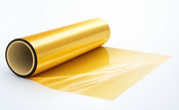
Source: Asahi Kasei
The film wasn't built from scratch. It fuses two technologies Asahi Kasei has sold for years: Pimel, its established photosensitive polyimide resin, and Sunfort, its photosensitive dry-film resist, which has a long track record in forming the fine copper structures inside chip packages. The targeted uses are the redistribution layer of semiconductor packages and the insulating layers of package substrates.
Why "film" beats "liquid"
Here is the crux of it. Insulating materials for chip packaging have traditionally been applied as a liquid: you spin a resin onto the surface, then bake it dry. That works well on a round silicon wafer. It works far less well on the large rectangular panels the industry is now moving toward.
A dry film solves that. With Asahi Kasei's product, the insulating layer is laminated onto the panel, pressed on like a sheet rather than spread on like paint. Lamination delivers an even coating across a big panel with consistent thickness, which matters enormously when packages need more and more stacked insulating layers. Asahi Kasei expects the approach to lift yields and productivity in panel-level packaging (PLP), the technique of building packages on large panels instead of round wafers.
If this "liquid becomes film" story rings a bell, it should. It is the exact playbook that made another Japanese material famous: Ajinomoto Build-up Film, or ABF. A seasoning company turned a liquid substrate insulator into a laminated film and ended up with a near-monopoly on a critical chip material. You can read how a food company came to own that corner of the chip industry in our earlier piece. Asahi Kasei is betting the same logic applies one layer up the stack.
It is worth being precise, though. Film is not simply replacing liquid. Asahi Kasei itself notes that as packages grow, the industry is weighing both liquid and film processes, and the company plans to serve both. Film is an option that gets more attractive the bigger the panel.
What polyimide actually does inside your AI chip
To see why this layer matters, picture the redistribution layer, or RDL.
An AI chip has thousands of microscopic input and output points crowded into a tiny area. They cannot connect directly to a circuit board, because the spacing is far too fine. The RDL is essentially a miniature, multi-layer wiring board built right onto the package. It "redistributes" those dense connection points, fanning them out to a workable size and routing signals between chiplets.
An RDL is a sandwich: layers of copper wiring separated by layers of insulating material. That insulator has a demanding job. It has to be an excellent electrical barrier, survive high processing temperatures, flex slightly without cracking, and allow extremely fine vias and lines to be patterned through it. Photosensitive polyimide is one of the workhorse materials for exactly that role.
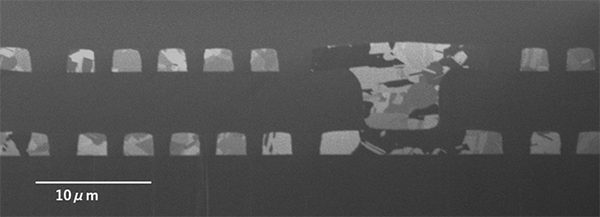
Source: Asahi Kasei
The more chiplets a package juggles, and the larger the panels get, the more RDL layers are needed, and the more it matters that each layer goes down flat, uniform, and free of defects. That is the specific pain point this film is designed to address.
Two technologies under one roof
Most materials suppliers specialize. One company is strong in insulating resins; another is strong in the resists used to pattern copper. Asahi Kasei's pitch is that it has both, and that fusing them is the whole point.
Alongside the new polyimide film, the company is promoting it as a pair with its Sunfort TA series, a high-performance dry-film resist rated for line/space patterns of 2/2 micrometers or finer, and demonstrated at 1.0 micrometer line width under laser direct imaging. A micrometer is one-thousandth of a millimeter. Combine the two, and a manufacturer can build both the fine copper circuitry and the insulating resin layer with a film-based lamination process, instead of juggling separate liquid and dry steps. A related Sunfort line, the CX series, handles the tall copper "pillars" needed for 3D stacking.
The strategic message is simple. Asahi Kasei isn't selling a single material. It is selling a panel-level process toolkit.
Who else is in this race
Photosensitive polyimide for packaging is a small but fiercely contested market. Estimates of its size vary widely between research houses, from roughly 600 million to 1.8 billion dollars a year, with projected growth anywhere from the low teens to above 20% annually. The one thing they agree on is the direction: up, in step with advanced packaging.
The established names are worth knowing. HD MicroSystems, a long-running joint venture rooted in America's DuPont and Japan's Hitachi Chemical, now Resonac, with operations in both countries, has for years been a reference supplier of RDL dielectrics for fan-out packaging. Toray, a Japanese materials giant, is generally cited by market researchers as the volume share leader. Fujifilm rounds out the Japanese contingent. Outside Japan, Kumho Petrochemical of South Korea and Eternal Materials of Taiwan are the main challengers.
Notice the pattern. Of the handful of companies that genuinely matter in this niche, three are Japanese, and a fourth is half-Japanese by ownership. Competition from the US and Korea is real. Korea in particular has pushed hard to localize chip materials since its 2019 trade friction with Japan. But at the leading edge, Japanese suppliers still tend to set the pace.
Why Japan keeps winning the materials game
Asahi Kasei's announcement is one tile in a much larger mosaic. Japan's grip on semiconductor materials, as opposed to the chips themselves, is one of the least-understood facts in tech. Silicon wafers, high-end photoresists, the ABF insulator, specialty cleaning chemicals: in category after category, Japanese firms hold dominant or near-dominant global share. We traced that broader picture in our look at how Japan's consumer-goods giants power the chip boom.
The reason isn't mysterious, and it isn't easily copied. Materials science rewards accumulated, hands-on knowledge, the kind built over decades of trial, failure, and close work with customers. Asahi Kasei's new film is a case in point. It didn't appear overnight; it grew out of the company's long histories in both Pimel and Sunfort. A rival can be funded generously and still discover it has bought time, not expertise.
That is also why this matters beyond Japan. As AI packaging turns into a chokepoint, every chipmaking region, from the US and Korea to Taiwan, Europe and China, has a strategic interest in not depending on a single country for its materials. Expect more localization drives, more consortiums, and more money. Whether anyone can close the gap is the open question.
What comes next
For now, Asahi Kasei's film is in customers' hands for evaluation, with commercialization as the next milestone. Its real test will be whether panel-level packaging takes off. The direction of travel is already visible: TSMC set up an R&D line for CoPoS, its next-generation Chip-on-Panel-on-Substrate platform, at subsidiary VisEra in 2025, with pilot production targeted for mid-2027. If panels do become the norm, the unglamorous business of laminating thin insulating sheets onto them could become one of the AI era's kingmakers.
In the AI economy, the spotlight lands on the chip designers and the cloud giants. But a surprising share of the real leverage sits with the companies making the boring-sounding stuff in between. Does your country have an industry like that: essential, globally competitive, and almost invisible to the public?








Global Discussion
5 comments