
⚡ A flash of light, less than two seconds, and the bottleneck of an entire memory technology is gone. That's what an Osaka University team has just demonstrated for magnetic tunnel junctions, the tiny devices at the heart of MRAM chips and ultra-sensitive magnetic sensors. The process that used to take a furnace several hours? They did it in 1.7 seconds.
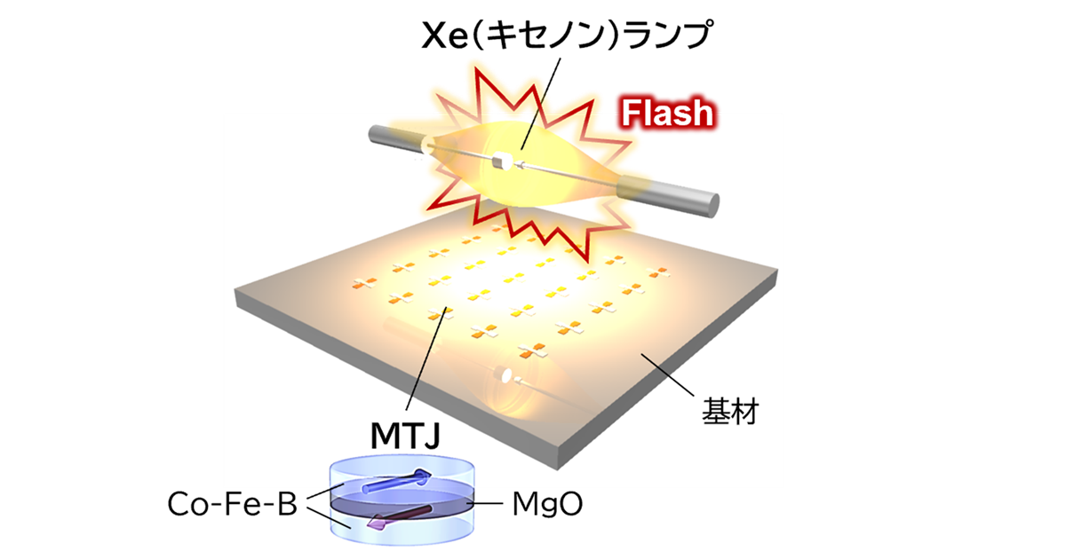
Source: Tohoku University / Osaka University press release
Why a memory most people have never heard of suddenly matters
Walk through any modern factory floor, data center, or, increasingly, the inside of a new car, and you'll find a quiet shift underway. The chips running edge AI, vehicle safety systems, and industrial controllers are starting to lean on a memory called MRAM, magnetoresistive random-access memory.
MRAM stores bits not as electric charges (the way DRAM and flash do) but as the magnetic orientation of a tiny stack of materials, called a magnetic tunnel junction, or MTJ. Two thin magnetic layers sandwich a barrier just a few atoms thick. Flip one layer's magnetization, and the resistance of the whole stack changes. That's how you read and write a bit.
The appeal: it's non-volatile (data survives power loss), endurance is essentially unlimited compared to flash, it tolerates radiation, and it's fast. Foundries have noticed. As of 2026, embedded STT-MRAM is in volume production at 22nm and 28nm nodes, primarily for automotive and IoT applications, with multiple foundries including Samsung, GlobalFoundries, and TSMC offering qualified processes. The STT-MRAM market is estimated at around $7.9 billion in 2026.
But MRAM has a quiet problem, and it shows up in the fab, not the spec sheet.
The annealing bottleneck
To make a working MTJ, you don't just deposit the layers. You have to bake them. That step is called annealing. It's needed to crystallize the layers properly and achieve a high tunnel magnetoresistance (TMR) ratio, the figure of merit that determines whether the device is usable at all. Conventional thermal annealing in a furnace typically takes several hours, including heating and cooling.
Industry-standard recipes generally call for 300–500 °C, held for tens of minutes to a few hours. On top of that, the MgO barrier at the core of the MTJ has to be deposited with 0.01 nm precision to repeatedly hit the targeted resistance and TMR characteristics. The thermal step is, in industry-speak, "rate-limiting", a single process that throttles the throughput of an otherwise modern line.
This matters because MRAM's economic competitiveness depends partly on bringing down its cost gap with flash and DRAM. Today the cost premium for embedded STT-MRAM over embedded flash sits at roughly 1.5–2×, narrowing but still real.
If you could cut the annealing step from hours to seconds, and do it without damaging the substrate, you'd change the calculus for an entire generation of devices.
What the Osaka team actually did
The group is led by Akiko Imai (assistant professor at Osaka University's Institute of Scientific and Industrial Research) and Daichi Chiba (professor at Osaka, who also directs Tohoku University's International Center for Synchrotron Radiation Innovation Smart Research Center, or SRIS). They worked with Teppei Araki, Tsuyoshi Sekitani, Jun Yamasaki of Osaka's Research Center for Ultra-High Voltage Electron Microscopy, and several other co-authors.
Their technique is called flash lamp annealing, or FLA. It's not new in semiconductor processing, it's been used for things like ultra-shallow junction formation in silicon, but applying it to MTJs is novel. The setup is conceptually simple: a xenon arc lamp fires millisecond-long pulses of intense, broadband light directly at the device surface. The MTJ absorbs the energy almost instantaneously.
The pulses can raise the surface temperature past 1000 °C in simulations, on timescales far shorter than those achievable with either conventional thermal annealing (CTA) or rapid thermal annealing (RTA). By repeating the pulses, the team reached a TMR ratio of about 100%, comparable to standard furnace annealing, in roughly 1.7 seconds total. That's up to several thousand times faster than the conventional process.
The result was published in npj Spintronics on May 12, 2026.
Source: Tohoku University press release
Why "fast" also means "less diffusion"
Speed isn't the only thing that changed. The team used transmission electron microscopy and energy-dispersive X-ray analysis to look at the atomic structure after FLA, and they noticed something interesting: the diffusion of boron atoms out of the CoFeB magnetic layer behaved differently than under conventional annealing.
That's a subtle but important point. In a furnace, you can't easily decouple "crystallize the right things" from "let everything else diffuse around." Tens of minutes at 400 °C will do both. With millisecond pulses, the heat is in and out before slower diffusion has time to take over. Because heat is generated within the surface and thin layer, this method allows the annealing of thin films, even on temperature-sensitive substrates, without damage to the substrate itself.
In practical terms: you can crystallize what you want, suppress what you don't, and leave the layer underneath cool enough to survive the experience.
The TSMC, Samsung, Everspin landscape, and where this fits
A breakthrough in fundamental processing doesn't slot into the foundry roadmap overnight. But the timing is interesting.
TSMC qualified its 22nm embedded MRAM platform for volume production in 2024, and the company has 16nm ready for customer verification with 12nm and 5nm versions in R&D. Samsung is targeting 8nm eMRAM by 2026 and 5nm by 2027. Standalone MRAM maker Everspin is on a different trajectory, it just signed a 10-year manufacturing agreement with Microchip Technology to expand onshore US production capacity, while its 256Mb xSPI STT-MRAM is scheduled to complete full production qualification in July 2026.
None of these companies are likely to swap their annealing tools tomorrow. Flash lamp annealers exist commercially, Japan's SCREEN Semiconductor Solutions makes the LA-3100, which already uses millisecond xenon pulses for dopant activation in advanced logic, but integrating FLA into a qualified MRAM line means re-doing reliability tests, AEC-Q100 automotive validation, and customer requalification. That's a multi-year process.
What the Osaka result does is shift the possibilities. If FLA can produce MTJs that meet or exceed conventional TMR ratios while letting you build on substrates that can't handle a multi-hour bake, flexible plastics, biocompatible materials, even paper-thin polymer films, you open product categories that simply aren't viable today.
The flexible-sensor angle
Here's where the story gets less abstract. The same Osaka group has been developing what they call "spin strain sensors", MTJ-based gauges that can achieve 500 times the sensitivity of conventional metal-foil film-type strain gauges that are widely used. The catch has been that you can't easily put them on flexible plastic substrates, because the substrate melts long before a furnace finishes annealing the MTJ.
FLA changes that. A millisecond pulse heats the top thin film without ever raising the substrate's bulk temperature significantly. Suddenly the same magnetic sensors that work on silicon could, in principle, sit on a wearable patch, a structural-health monitor wrapped around an aircraft wing, or a soft robotic skin.
That's still in the research phase. But it's the kind of secondary application that often ends up being more disruptive than the headline use case.
Japan's quiet spintronics legacy
It's worth noting where this fits in a longer story. Japan punches above its weight in MRAM fundamentals despite trailing Taiwan and South Korea in semiconductor manufacturing overall. The MgO tunnel barrier that almost every modern MRAM cell uses traces back to a 2004 Nature Materials paper led by Shinji Yuasa at AIST. Voltage-controlled magnetic anisotropy (VCMA), which enables electric-field-assisted switching in STT-MRAM, can reduce write current requirements by 30–50% compared to conventional current-only switching, that line of research also has deep Japanese roots.
Tohoku University runs one of the world's most active MRAM research centers. AIST has been pushing voltage-driven MRAM. Now Osaka adds the manufacturing-process angle. It's a coordinated, if uncoordinated, push that keeps showing up at the front of the field.
What's still uncertain
A few honest caveats before anyone calls this revolutionary.
The result is a research demonstration, not a production-qualified process. The team showed about 100% TMR, solid, but state-of-the-art industrial MTJs reach considerably higher ratios. Scaling FLA across 300mm wafers with uniformity, repeatability, and the yield numbers a foundry needs is a separate engineering problem. And while the boron-diffusion difference is interesting, the full physics of crystallization under non-equilibrium millisecond heating still needs to be mapped out. The group plans further structural analysis at synchrotron facilities.
There's also a competitive question. Flash lamp annealing has been studied for semiconductor processing for over two decades, and major equipment vendors have mature tools. Whether Japanese, Taiwanese, or US players move first to integrate FLA into MRAM lines will depend less on the underlying science than on which fab is willing to absorb the qualification cost.
The bigger picture
Memory technology often looks boring from the outside until the moment it isn't. Flash storage was a curiosity in the 1990s and a $90 billion industry by 2020. MRAM has been called the "next big thing" for so long that the phrase has lost meaning. But the trajectory is now plausible: foundries scaling embedded MRAM to leading-edge nodes, standalone densities pushing toward 1 Gb, AI accelerators looking for non-volatile on-chip memory.
If the annealing step really can collapse from hours to seconds without compromising device quality, the case for putting MRAM almost everywhere, wearables, vehicles, satellites, AI inference chips, gets meaningfully stronger.
How fast that translates to a chip in your phone is anybody's guess. But the bottleneck just got a lot smaller.
How is research and manufacturing for next-generation memory progressing in your country? Are universities or government labs pushing similar process-level breakthroughs? Tell us in the comments.
References
- Tohoku University press release (May 13, 2026): https://www.tohoku.ac.jp/japanese/2026/05/press20260513-01-MTJ.html
- Imai, A., Ota, S., Yamasaki, J., Araki, T., Kanai, Y., Koyama, T., Sekitani, T., & Chiba, D. "Ultrafast flash lamp annealing of magnetic tunnel junctions." npj Spintronics (2026). DOI: https://doi.org/10.1038/s44306-026-00145-z
- EE Times Japan: https://eetimes.itmedia.co.jp/ee/articles/2605/20/news033.html
- Everspin Technologies, Microchip manufacturing agreement: https://investor.everspin.com/news-releases/news-release-details/everspin-technologies-expands-shore-mram-manufacturing-capacity
- Samsung Semiconductor, eMRAM roadmap: https://semiconductor.samsung.com/news-events/tech-blog/developing-the-industrys-most-energy-efficient-next-generation-mram-selected-as-iedm-highlight-paper/








Global Discussion
5 comments