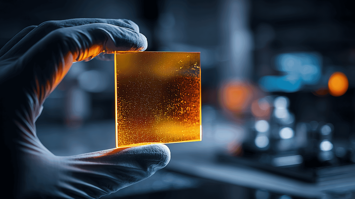
What if the world's hardest material could also become the world's most advanced semiconductor? A Tokyo-based company known for processing gemstones has just produced a 30mm square (111) diamond wafer, roughly the size of a postage stamp but ten times larger than anything the industry could make before. This tiny leap is a giant one for quantum sensors, power chips, and even space electronics.
Diamond Substrates: Orbray's World-First Leap
On April 15, 2026, Orbray Co., Ltd., an 87-year-old Tokyo company formerly known as Adamant Namiki Precision Jewel, announced that it has successfully produced a 30mm square freestanding (111) single-crystal diamond substrate, the largest ever made in the world. The achievement was documented in a peer-reviewed paper published in Applied Physics Express on March 11, 2026.
To put the number in perspective: until recently, the (111) diamond substrates available to researchers were typically just a few millimeters on a side, about the width of a grain of rice. Orbray jumped to 20mm square in March 2025, and has now pushed that frontier to 30mm square in just over a year. For a material notorious for resisting being grown in any meaningful size, this is a remarkable pace.
Why (111) Matters: The Quiet Star of Crystal Faces
Diamond, like most crystals, can be cut along different atomic planes. The two most important for semiconductors are the (100) face and the (111) face. They look almost identical to the naked eye, but behave very differently at the atomic level.
The (100) face is the workhorse. It's easier to grow cleanly, and industry has used it for years in grinding wheels, cutting tools, and early power-semiconductor research.
The (111) face is harder to make but more powerful. It has two properties that the (100) face can't match:
- Easier n-type doping. Semiconductors need both "n-type" and "p-type" regions to function, much like how a battery needs both a plus and minus terminal. Diamond has historically been very difficult to convert to n-type. The (111) face makes this crucial step much more tractable.
- Aligned NV-center spins. The (111) orientation naturally aligns the spin axes of nitrogen-vacancy (NV) centers, microscopic quantum defects that can be used as exquisitely sensitive magnetometers or quantum memory units. For quantum sensing, this alignment is not a nice-to-have; it's essential.
In short, (111) diamond is the key that opens doors both to better power chips and to practical quantum devices. The only problem: nobody could make it in useful sizes. Until now.
The Twin Problem: How Orbray Cracked It
The specific obstacle was a crystal defect called a twin. In English, a "twin" crystal is a region where the atomic lattice suddenly flips into a mirror-image orientation. On (111) diamond, twins appear so readily that larger wafers quickly become patchworks of mismatched domains, useless for high-precision devices.
Orbray's team grew their diamond on a sapphire substrate coated with a thin buffer layer of iridium, using microwave plasma chemical vapor deposition (MPCVD), a technique where methane and hydrogen gas are energized into a plasma, and carbon atoms settle onto the sapphire one layer at a time.
The breakthrough came from a surprising variable: the tilt angle of the sapphire base. By using sapphire substrates that were steeply misoriented from the standard (0001) plane, and specifically tilted along the <11-20> direction, the researchers found that diamond atoms arranged themselves into orderly "step-flow" growth patterns, essentially, atoms climbing a staircase instead of piling up randomly. This geometry mechanically suppressed twin formation across the entire 30mm square area. X-ray diffraction measurements confirmed a single-crystal structure over the full substrate, with no detectable twinning.
It's the kind of result that looks obvious in hindsight but required years of patient materials-science detective work.
The Quantum Sensor Connection
Outside power electronics, the most exciting application may be quantum sensing.
An NV center is a nitrogen atom paired with a missing carbon atom next to it, sitting inside the diamond lattice. It's a defect, but a useful one: the electron it hosts responds to magnetic fields, electric fields, temperature, and strain with astonishing precision. NV-center magnetometers can already detect the magnetic fields generated by a single neuron firing inside a living brain, or map the tiny magnetic signatures of geological samples.
The catch is that you need lots of NV centers, all pointing the same way, to get a good signal. Random orientations average out to nothing. The (111) face naturally aligns NV centers perpendicular to the surface, so a (111) wafer gives you a whole sheet of cooperating quantum sensors.
Switzerland's Qnami, Germany's NVision Imaging, and several Japanese firms are already racing to commercialize NV-center devices for biomedical imaging, battery diagnostics, and brain-computer interfaces. A 30mm square (111) wafer makes the economics work for the first time.
Orbray: From Gemstones to Quantum Materials
Orbray's backstory is worth knowing. Founded in 1939 as a jewel-bearing manufacturer for mechanical watches and measuring instruments, the company spent decades perfecting the art of cutting, shaping, and polishing small gems. That hard-won expertise in working with ruby, sapphire, and eventually synthetic diamond is the foundation of what you're reading about today.
The company rebranded from Adamant Namiki Precision Jewel to Orbray in 2023. With roughly 2,300 employees and approximately $192 million in consolidated revenue in its most recent fiscal year (¥30.6 billion at the current exchange rate of about ¥159 per US dollar), it is still modest by semiconductor-industry standards. But its technology portfolio is unusually deep: large-diameter synthetic diamond, 12-inch sapphire (a world first when announced in 2022), precision jewel components, micro DC motors, medical device parts, and optical communication components.
In 2022 it became the first company to mass-produce 2-inch ultra-pure diamond wafers, a milestone aimed at quantum computing applications. In 2024 it announced a partnership with UK-based Element Six, the world's other heavyweight in synthetic diamond, to jointly develop large-diameter single-crystal diamonds. Orbray is, quietly, one of the most important companies in the global quantum and power-semiconductor material supply chain.
Why Japan Is Leading This Race
Diamond semiconductor development is one of the few high-technology areas where Japan has a clear, durable lead. Orbray supplies the wafers. Startups like Power Diamond Systems and Diamond Semiconductor (a Saga University spinoff) build the devices. Universities and national labs, Waseda, Saga, Kanazawa, NIMS, AIST, contribute fundamental research. Okuma Diamond Device in Fukushima Prefecture is building the world's first diamond-semiconductor mass-production facility. Government funding through NEDO knits it all together.
The ecosystem is unusually tight for such a niche field, and it's the product of more than 30 years of patient public investment. For related context on the device side of the story, see our earlier coverage of Power Diamond Systems' world-first 200V/1A switching and the subsequent DC-DC converter demonstration, both of which rely on material supplied by companies like Orbray.
The Road Ahead
Orbray says the next steps are further scaling, improving crystal quality, and producing doped (111) substrates ready for device fabrication. Real-world applications will arrive in waves: first high-sensitivity quantum sensors and extreme-environment electronics (satellites, nuclear facilities), later mainstream power devices for EVs, renewable energy, and data centers.
There are still formidable challenges. Diamond remains expensive to process because it is, famously, the hardest material on Earth. Wafer sizes, though growing, remain far behind silicon's 300mm (12-inch) and even silicon carbide's 200mm (8-inch) standards. And the global diamond-semiconductor industry is still young enough that supply chains, standards, and customer confidence all need to be built from the ground up.
But for the first time, the material side of the equation, the thing that has been holding back diamond electronics for decades, is starting to catch up with the demand.
What's It Like in Your Country?
In Japan, diamond is quietly shifting from "jewelry" to "industrial foundation." Research labs, startups, and century-old companies are all converging on the same strange, brilliant material.
In your country, is diamond being discussed as a semiconductor material? Are there quantum-sensor programs, power-device research efforts, or university groups working in this space? What role do you think diamond will play in your nation's technology future? We'd love to hear your perspective.







Global Discussion
0 comments