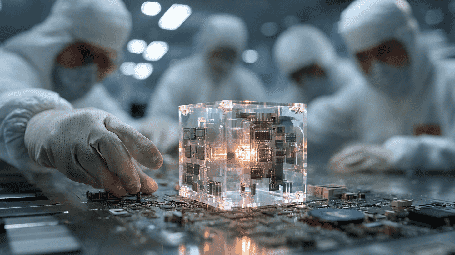
Resonac, the world's leading supplier of back-end semiconductor materials, formed in 2023 by merging Showa Denko and the old Hitachi Chemical business, has fully launched US-JOINT, a 12-company Japanese-American R&D consortium, at a new facility in Union City, California. On April 20, 2026, public and private officials from both countries gathered for an opening ceremony that marks the first consortium in the United States dedicated exclusively to advanced semiconductor packaging.
The stated goal is blunt: get into the design rooms where Google, Apple, Meta, Amazon, Microsoft, Broadcom, and AMD are sketching their next custom AI silicon, and make sure those chips are assembled with Japanese materials.
Why back-end is the new battlefield
Chipmaking splits into "front-end" (etching circuits onto silicon wafers) and "back-end" (dicing the wafers and assembling the final package). As Moore's Law scaling hits physical limits, most of the remaining performance headroom has migrated to the back-end.
NVIDIA's GPUs and AMD's data-center accelerators are the template. Instead of one giant die, they stack GPU logic chips next to high-bandwidth memory (HBM) and link them through silicon interposers or bridges. TSMC's CoWoS (Chip on Wafer on Substrate) is the best-known flavor of this "chiplet" architecture, and it has become the rate-limiting step for generative AI throughput.
What matters for Resonac's play is that advanced packaging is not one product, it is a recipe. Insulating films, die attach films, mold compounds, CMP slurries, photoresists, sputter and ashing tools, laser dicing, flux-free thermocompression bonders: each comes from a different supplier, and each has to be re-tuned for every new chip design.
What US-JOINT actually is
The 12 members are Resonac plus KLA (inspection and laser direct imaging), Kulicke & Soffa (flux-free thermocompression bonding), Moses Lake Industries (high-purity chemicals), MEC (copper surface treatment), ULVAC (sputtering and ashing), NAMICS (liquid encapsulants), TOK (photoresists), TOWA (the world's top compression molding equipment maker by share), Toppan (FC-BGA substrates and interposers for high-end data centers), Azimuth, and 3M (advanced materials and adhesives). Five US firms, seven Japanese firms.
Materials suppliers normally guard their recipes fiercely, the difference between a functional dielectric and a useless one often comes down to a fraction of a percent of a proprietary additive. US-JOINT's novelty is that it deliberately lowers those walls. Each member installs its latest materials and tools in one shared cleanroom, and hyperscaler engineers are invited in to prototype and validate new package concepts side by side with the chemists who formulated the films.
Hidehito Takahashi, Resonac's CEO, said at the opening that the consortium aims to cut proof-of-concept cycles from roughly six months to as little as one. An 83% compression is what the generative AI cadence demands.
Why the trip to Silicon Valley was necessary
The obvious question: Japanese suppliers were already embedded in the global chip supply chain. Why build a physical outpost in California?
The answer is that design intent now originates in a different zip code than it used to. Chip architectures used to be dictated by Intel or TSMC's customers. Today the loudest voices in the room are GAFAM and the AI accelerator companies, who design silicon around the exact needs of their cloud services and foundation models. When a Google or Meta engineer sketches a new interposer concept on Monday, the Japanese materials supplier whose film gets specified on Friday matters enormously.
Six-month round-trips of samples from Kawasaki to Santa Clara simply cannot keep up. Being in the same time zone, the same meeting room, the same lunch line is the whole point. Dilip Vijay, Broadcom's VP of Global IC Operations, publicly said this kind of collaboration is "exactly what the industry has needed."
A three-story consortium structure
US-JOINT did not appear overnight. It extends domestic Japanese consortiums called JOINT (launched 2017) and JOINT2 (14 Japanese companies), which have already prototyped a chip-embedded interposer on 510×515 mm panels carrying 20 bridge dies apiece. That program targets commercialization in 2027–2028. In September 2025 a third tier, JOINT3 (27 members), was added for still-earlier-stage research.
In other words, Resonac is running a pipeline: JOINT3 explores raw concepts, JOINT2 prototypes on large panels inside Japan, and US-JOINT translates those capabilities into whatever the American hyperscalers actually want to build. JX Advanced Metals (sputtering targets), OKUNO Chemical (plating chemicals), and a deep bench of other "world-top-share-but-you've-never-heard-of-them" Japanese suppliers sit behind the curtain.
Who is Resonac, anyway?
If the name is new to Western readers: it is the company formed in January 2023 when Showa Denko absorbed its Showa Denko Materials subsidiary (the old Hitachi Chemical electronic materials business). The combined semiconductor and electronics unit generates roughly ¥400 billion (about US$2.5 billion at ¥159 to the dollar) per year, a little over 30% of group revenue, and holds the number-one global share in several back-end material categories: CMP slurries, copper-clad laminates, photosensitive films, die attach films, and high-purity gases among them.
Any single one of those materials sounds mundane. In aggregate, they mean that almost every advanced AI chip rolling out of a Silicon Valley design studio has Japanese materials somewhere in its physical build.
Open questions
US-JOINT is not guaranteed to succeed. Broadcom and AMD were introduced at the ceremony as stakeholders, not as formal consortium members, and how their feedback will be systematically fed back into development remains unclear. Twelve companies in partly overlapping competitive spaces will need unusual discipline about what intellectual property to pool and what to keep. And TSMC's CoWoS remains the king of advanced packaging, US-JOINT's realistic position is probably to offer an alternative packaging path to US hyperscalers rather than to displace the Taiwan incumbent.
Resonac has not disclosed a budget figure for the initiative. The degree of CHIPS Act alignment and Japanese government co-funding will likely become clearer over the next fiscal year.
The bigger picture
"A Japanese-American back-end packaging R&D lab just opened in the Bay Area." Read at surface level, that is a dull sentence. Read properly, it means the place where GAFAM's next generation of AI silicon will get its physical form has moved a few miles inland from Oracle Park, and the dominant voice in the room on the materials side is Japanese.
Front-end lithography belongs to ASML. Leading-edge foundry belongs to TSMC. Deposition and etch belong to Applied Materials and Lam Research. Back-end materials, increasingly, belong to Resonac and its Japanese collaborators. Semiconductor supremacy has long since stopped being a national contest; it is now a stack of specialist companies each holding one layer. What just changed is that the Japanese layer got a permanent seat at the Silicon Valley table.
Does your country have this kind of quiet industry leader, the company nobody outside the sector has heard of, but without which nothing works? Japan has a whole genre of these, and we'd love to hear what the equivalent looks like where you live.






Global Discussion
14 comments