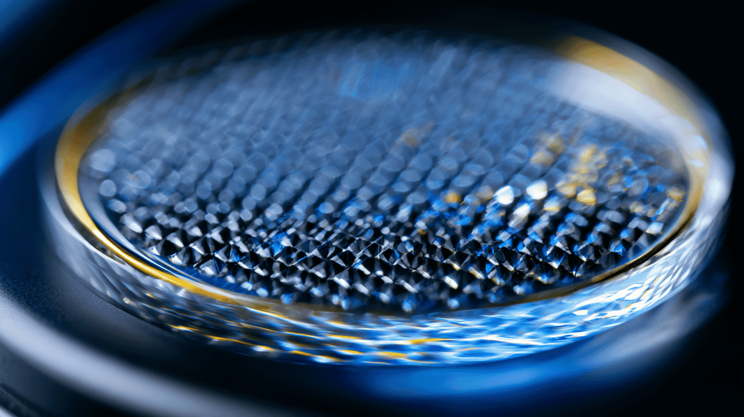
💎 Diamond has long been called the ultimate semiconductor material. One of its hard problems has been getting it to switch off reliably. On September 18, 2026, Kanazawa University and Japan's National Institute of Advanced Industrial Science and Technology (AIST) said they had run the first vertical diamond transistor that switches off the same way a silicon one does.
Switching off comes first
Inside an electric vehicle's motor drive or a power grid, power semiconductors (chips built to handle large amounts of electricity) act as switches, turning current on and off. The workhorse is the MOSFET, a transistor whose current is controlled by the voltage on its gate.
For this job, one property is essential: being "normally-off." With no voltage on the gate, no current flows. The opposite, a "normally-on" device, conducts unless you actively hold it shut.
A normally-off device behaves like a faucet that closes when you let go of the handle. A normally-on one springs fully open instead. If a control circuit fails or the power cuts out, the first stops the flow by itself and the second keeps it running. That is why equipment handling large amounts of power calls for the first kind.
Diamond's physical properties suit this work. Its bandgap, a rough measure of how well it resists leaking current, is about 5.5 eV, against 3.2 to 3.4 eV for silicon carbide (SiC) and gallium nitride (GaN), and 1.1 to 1.2 eV for silicon. According to a 2016 announcement, it conducts heat 14 times better than silicon. It tolerates high voltages and sheds heat easily, which on paper means doing the same work with a smaller chip.
There was more than one way to switch diamond off
The type studied most widely around the world uses a diamond surface coated with hydrogen, known as hydrogen termination. A conducting path forms on that surface naturally, and that path is why these devices are basically normally-on.
At least two other routes already existed. One comes from Power Diamond Systems (PDS), a startup founded on research from Waseda University, which caps the surface with silicon oxide (C-Si-O termination). In December 2023, the company announced that joint research with Waseda had made both lateral and vertical devices normally-off this way.
The other is the "inversion-layer channel" this research group uses. A conducting path, the inversion layer, appears at the surface only when voltage is applied to the gate. It is the same principle as a silicon MOSFET: with no voltage, the path simply does not exist, so off is the default state. In 2016, working with the auto parts maker Denso, the group ran the first lateral device of this kind and published it in Scientific Reports.
The new "world first" builds on that. According to the team, it is the first demonstration of a vertical diamond MOSFET with an inversion-layer channel.
A switch built into the walls of a pit
In diamond, an inversion layer forms only on the crystal's {111} faces, one particular orientation of the lattice. A vertical trench device puts its switch on the side walls of a carved pit, so those walls have to be clean {111} faces. Conventional etching could not deliver that, so no vertical inversion-channel device had worked until now.
The group's method dissolves diamond's carbon into nickel in high-temperature steam, with no chemicals or plasma involved. The reaction slows almost to a halt on {111} faces, so everything else is eaten away first and the {111} faces are left standing as walls. On a flat (100) surface, the result is a row of inverted-pyramid pits with {111} sidewalls.
A device using those walls as its channel showed clear transistor behavior at room temperature and at 300°C, and stayed normally-off. The paper went online on September 4, 2026, in the journal Diamond and Related Materials. The co-first authors are Yuto Nakamura, a doctoral student at Kanazawa University, and Masatsugu Nagai, a researcher at AIST. The group is led by Norio Tokuda, a professor at Kanazawa University's Diamond Research Center.
Why power chips go vertical
A lateral device, which sends current sideways along the chip, is simple and easy to make. But design it to withstand high voltage and its resistance per unit area climbs steeply. That makes it a poor fit for power devices.
Vertical devices send current down through the thickness of the chip, and they come in two kinds. Planar devices put the switch on a flat surface. Trench devices put it on the walls of pits. Trenches pack more switching area into the same footprint and avoid a loss mechanism that planar designs suffer from, called JFET resistance. The press release describes the trench as the lowest-loss layout. This group jumped from lateral straight to trench, skipping planar entirely.
In SiC, ROHM started mass-producing SiC MOSFETs in December 2010 and trench SiC MOSFETs in June 2015, calling both a world first. Even for a company already making SiC MOSFETs in volume, reaching trench production took five years.
What comes after the wafer
We covered the push to make diamond wafers bigger earlier. In June 2026, Tokyo-based Orbray and Element Six, part of De Beers Group, established production technology for 3-inch single-crystal diamond. Their 2-inch wafers are in the final stage of mass-production preparation, and development has started on 4-inch crystals that fit existing semiconductor lines. But a bigger wafer is not a product without a device on top of it that switches off safely.
The press release gives no figures for breakdown voltage, current, or on-resistance. The team's own stated next step is to optimize the structure and cut losses further. Electric vehicles and power grids appear only as eventual hopes. Part of the work was funded by NEDO (Japan's New Energy and Industrial Technology Development Organization), the Japan Society for the Promotion of Science, and the Japan Science and Technology Agency (JST).
In France, Diamfab, a 2019 spin-off of the national research agency CNRS in Grenoble, is working with Schneider Electric and others on DIAMSHIELD, a project started in 2025 to develop diamond transistors for smart grids. Which path reaches a product first, hydrogen termination, silicon-oxide termination or the inversion layer, nobody can yet say.
What material do you expect to run the next generation of power electronics where you live?
References
- https://www.kanazawa-u.ac.jp/press/187580/
- https://www.kanazawa-u.ac.jp/wp/wp-content/uploads/2026/09/20260918.pdf
- https://doi.org/10.1016/j.diamond.2026.114141
- https://www.jst.go.jp/pr/announce/20160822/index.html
- https://www.waseda.jp/inst/nanolife/assets/uploads/2023/12/f82fbebc5f8d9308fb2e0b1d3c987e9b.pdf
- https://emira-t.jp/ace/24422/
- https://fscdn.rohm.com/jp/products/databook/catalog/common/SiC_PowerDevices_JP.pdf
- https://monoist.itmedia.co.jp/mn/articles/2607/02/news011.html
- https://kyodonewsprwire.jp/release/202406112001
- https://www.minalogic.com/wp-content/uploads/2024/12/pr-diamfab.pdf
- https://euraxess.ec.europa.eu/jobs/353194







Global Discussion
4 comments