In the late 1980s, Japan made more than half of the world's semiconductors. Today its share is below 10%.
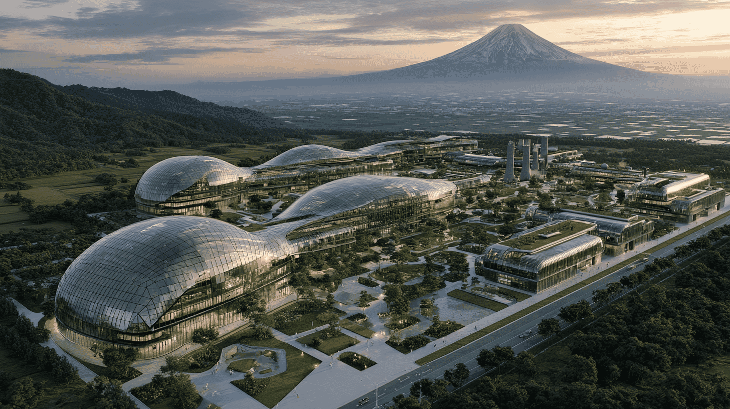
Now a state-backed comeback is taking shape in the rice fields of southern Japan. On April 27, 2026, Kumamoto Prefecture, the city of Koshi, and real-estate giant Mitsui Fudosan signed a partnership agreement to launch the "Kumamoto Science Park", a roughly 31-hectare site (about 6.5 Tokyo Domes, or 76 acres) right next to TSMC's chip fabs, designed to anchor Japan's semiconductor revival by 2030. Modeled on Taiwan's legendary Hsinchu Science Park, the project aims to cluster industry, academia and government around 3-nanometer chip production. Here is what the plan actually contains, how it compares with the US CHIPS Act and the EU Chips Act, and the boom-and-strain dynamics already reshaping the region.
What was signed on April 27
The signing ceremony took place at Hotel Kumamoto Terrsa in central Kumamoto City. Three figures put their names to the document: Kumamoto Governor Takashi Kimura, Mitsui Fudosan's Solution Partner Division head Kyosuke Hosoda, and Koshi City Mayor Yoshiyuki Araki.
The three parties will collaborate on:
- Developing the core "Innovation Creation Area" in the Takeyusumi district of Koshi City, about 31 hectares.
- Recruiting companies, universities and research institutes into the zone.
- Establishing and operating a park-management entity.
The schedule is concrete. Site preparation begins in May 2026, facilities open in stages from 2027, and full completion is targeted for 2030.
Mitsui Fudosan says it will support the full pipeline from research and development through to mass production, with explicit reference to 3-nanometer-class chips. President Shun Ueda said in a statement that the company aims to "send a science park where new technology and businesses are born from Kumamoto to the world." Governor Kimura framed it more directly: "We want to give birth to the industries of the future from Kumamoto."
Location is the message: right next to TSMC
The chosen site in Koshi City sits immediately west of JASM, TSMC's Japanese joint venture with Sony, Denso and Toyota, and the existing Semicon Techno Park. A new Sony Semiconductor Manufacturing factory is going up nearby, and the Central Kyushu Cross-Country Highway is under construction within easy reach.
The geography itself is the strategy. Place R&D, talent development and startup activity within walking distance of the most advanced semiconductor fabs in Japan, and the spillovers compound.
The blueprint is borrowed from Taiwan's Hsinchu Science Park, TSMC's home turf, where chipmakers, suppliers, research institutes and universities have been packed together for decades. That density is widely credited with Taiwan's world-leading speed from technology development to commercial production. In July 2024, Mitsui Fudosan signed cooperation agreements with Taiwan's National Yang Ming Chiao Tung University and the Industrial Technology Research Institute (ITRI), preparing to transplant the Hsinchu DNA to Japan.
A "distributed park", not a Hsinchu copy-paste
What makes the Kumamoto plan distinctive is that it is officially a "distributed science park." The 31-hectare Koshi site is the core hub, but multiple zones across the prefecture will share specialized functions, networked together rather than concentrated in a single mega-campus.
Hsinchu is one large park. Kumamoto, constrained by available land and traffic infrastructure, is going for a multi-node model. Mitsui Fudosan executives have repeatedly emphasized that the project is "not just a factory recruitment exercise but a town-building one", housing, retail, workforce development and corporate ecosystems integrated into a single plan.
Why now: the state of "Hinomaru" semiconductors
Japan's chip industry once dominated. In the late 1980s, NEC, Toshiba, Hitachi and Fujitsu were household names in DRAM, and Japan held over 50% of the global semiconductor market. Then came the US-Japan trade frictions of the 1990s, missed investment cycles, and the global rise of the foundry-fabless split. Japan's share fell below 10%.
Two converging forces now create a window for revival.
First, AI demand. The boom around ChatGPT, NVIDIA GPUs and AI infrastructure has supercharged demand for cutting-edge logic chips. Second, geopolitical risk. The concentration of advanced manufacturing in Taiwan, against the backdrop of cross-strait tensions, has redefined chip capacity as a national-security issue worldwide. Japan's government has responded with a torrent of money: over 2.3 trillion yen ($14.5 billion at recent rates of about 159 yen to the dollar) cumulative support for Rapidus, the 2nm foundry under construction in Hokkaido; roughly 1.2 trillion yen ($7.5 billion) in subsidies between TSMC's first and second Kumamoto fabs; and the dramatic upgrade of Fab 2 from a 7nm-class plan to 3nm-class production.
The Kumamoto Science Park is the connective tissue this strategy needs. Factories alone do not sustain an industry. Materials, manufacturing equipment, design houses, packaging firms, talent pipelines and startups all have to cluster before an autonomous ecosystem can take root.
How it stacks up against the US CHIPS Act and the EU Chips Act
The world is now in an open subsidy race for semiconductors. Where does Japan's approach sit?
United States, CHIPS and Science Act (2022, roughly $76 billion total scope). Major manufacturing grants have flowed to TSMC Arizona, Intel Ohio, Samsung Texas and Micron New York, alongside a 25% investment tax credit for facility build-outs initiated by the end of 2026. The political environment under President Trump has been less friendly to the law, raising questions about continuity even as the projects themselves continue.
European Union, European Chips Act (in force since September 2023, around €43 billion / about $50 billion mobilization). Funding has gone to ESMC in Dresden (the TSMC-Bosch-Infineon-NXP joint venture), Infineon, STMicroelectronics, and a network of research pilot lines anchored by imec, CEA-Leti and Fraunhofer. The EU's stated goal is to double its global chip share to 20% by 2030, but industry voices are already calling for a "Chips Act 2.0," arguing the current design over-emphasizes sub-5nm cutting-edge chips relative to actual European demand.
Japan's twist. Japan combines two manufacturing pillars, recruiting an established global leader (TSMC Kumamoto) and incubating a domestic foundry (Rapidus), and now adds a third, place-based pillar: regional ecosystem zones like the Kumamoto Science Park. The total spending is smaller than the US headline figure, but Japan is concentrating its bets geographically and institutionalizing industry-academia-government coordination in a way few peers have matched.
The light and the shadow in Kumamoto
The TSMC effect is already visible in the numbers. The Kyushu Financial Group estimates a roughly 11.2 trillion yen (about $70 billion) economic ripple effect for Kumamoto Prefecture between 2022 and 2031, with the wider Kyushu region potentially reaching 20 trillion yen.
But the boom has a shadow. Industrial land prices in neighboring Kikuyo Town jumped 32% in a single year, the largest increase in Japan in 2022. Rents in the area have doubled or tripled in some pockets, with reports of supermarkets closing because they could not absorb the increases. The effective jobs-to-applicants ratio for semiconductor manufacturing roles in Kumamoto rose from 0.56 in fiscal 2020 to 3.33 in fiscal 2021. Forecasts suggest Kyushu will be short roughly 1,000 semiconductor-related workers per year for the next decade.
The labor crunch radiates outward. Hourly wages needed to recruit staff in restaurants, cleaning and logistics have climbed by roughly 50%. Local small and mid-sized firms cannot match TSMC-level packages and are losing engineers. Concerns about groundwater consumption and wastewater discharge, heavily regulated under Kumamoto's groundwater preservation ordinance, also continue to surface in local debates.
The Science Park lands on top of this terrain. It is expected to lift wages and employment further; it will also raise pressure on local infrastructure and small-business survival. Coexistence policy will matter as much as technology policy.
Voices from the trade-show floor: the case for domestic chips
The agreement was announced on the same day a major technology trade show opened in Kumamoto, drawing more than 700 exhibitors from Japan and abroad. Visitors saw a vehicle-shaped robot transform into a humanoid in under a minute, a humanoid named "cinnamon1" that responds to gesture cues, and a robotic arm that throws pottery with delicate finger control.
Taisuke Ono, CEO of humanoid developer Donut Robotics, told reporters that his company has an ambition to make every component domestically: "I really want Japanese semiconductor makers to step up." Yusuke Fujiwara, an executive officer at Highlanders, which builds Japanese-developed AI robots, welcomed the news, saying it is "very encouraging" that domestic chips are becoming a real option.
For Japanese frontier-tech companies in robotics and AI, supply-chain risk, including hacking and conflict-driven cutoffs, is not abstract policy. It is a daily product-design decision. The Science Park is, among other things, an answer to those concrete industrial worries.
The road to 2030
Three challenges loom.
First, attracting tenants of the right caliber. Hsinchu thrived because TSMC's headquarters was rooted there. JASM in Kumamoto is, structurally, an outpost of a Taiwan-based parent. Building genuinely local R&D substance, rather than just hosting branch labs, will be the harder achievement.
Second, the human pipeline. Partnerships with Kyushu University, Kumamoto University, NYCU and ITRI have to translate into talent programs that actually produce engineers at the rate the cluster needs.
Third, coexistence. Land prices, traffic, groundwater, agriculture, the friction is already real, and the Science Park will amplify all of it before it eases anything.
By 2030, when the full complex is set to be done, will "Hinomaru" semiconductors have a comeback story? The Park is the box; companies, researchers, engineers and residents will determine the contents.
Japan is now navigating a tangled mix of subsidy strategy, real-estate pressure, talent shortages and ecosystem design. How does your country position semiconductors, and what is the strategy where you live? Tell us in the comments.
References
- Kumamoto Science Park concept announced (TBS NEWS DIG via Yahoo!)
- Kumamoto Prefecture, Mitsui Fudosan and Koshi City sign agreement (Kumamoto Nichinichi Shimbun via Yahoo!)
- Mitsui Fudosan partnership agreement on Kumamoto Science Park (Nikkei)
- Mitsui Fudosan Science Park Kumamoto Project (official site)
- Kyushu semiconductor "Science Park" plan (Nikkei xTECH)








Global Discussion
0 comments