
💎 The world's first factory built to mass-produce diamond semiconductors just opened, and of all the places it could have been, it stands in Okuma, the Fukushima town that hosts the wrecked Daiichi nuclear plant. The story of how a material scientists chased for forty years, with almost nothing to show for it, ended up here is really a story about what disasters leave behind.
A material with no use
For most of its life as a research subject, the diamond semiconductor was an answer waiting for a question.
The physics is remarkable. Diamond moves heat better than any other material, barely flinches under radiation, and keeps working at voltages and temperatures that would cook an ordinary chip. Japanese labs have known this since the 1980s. A turning point came in 1982, when the institute now part of NIMS (Japan's National Institute for Materials Science) pioneered a way to grow synthetic diamond by chemical vapor deposition: feeding methane and hydrogen into a chamber and coaxing solid diamond out of the reaction.
And then, for a long time, not much happened. The properties were extraordinary in ways that no commercial market actually needed. Silicon was cheap and good enough for almost everything. Diamond, meanwhile, was punishing to work with: the very hardness that makes it precious makes it miserable to shape into a clean, usable wafer. So the research stayed quiet, passed from one institute to the next like a relay run by people who believed the payoff would come without knowing when, or whether, it would. For decades it never left the lab.
The disaster that gave diamond a job
What changed everything was the worst day in modern Japanese memory.
On March 11, 2011, a magnitude-9 earthquake and the tsunami that followed triggered a triple meltdown at the Fukushima Daiichi plant. The cleanup that began afterward is one of the hardest engineering challenges anyone has taken on. The most daunting part is retrieving the fuel debris: the mass of melted nuclear fuel fused with reactor structure, sitting in radiation so intense that silicon-based electronics fail within a short time of being lowered inside.
Suddenly, a material that "doesn't break under radiation" wasn't an academic curiosity. It was a requirement.
In 2012, the year after the accident, a national project formed to develop diamond semiconductors specifically for this fight. The Japan Atomic Energy Agency (JAEA) led it; AIST, Hokkaido University, NIMS and the high-energy physics lab KEK joined in. For the first time, the know-how that had been scattered across separate institutes for thirty years had a reason to converge. And it did. A clear, brutal, real-world deadline turned a slow research relay into a sprint.
The entrepreneur who spent six years saying "not yet"
Most stories like this end in a journal paper. This one needed someone who could carry a national project across the gap into a company that ships actual hardware, and for years no one filled that role.
Naohisa Hoshikawa, a Hokkaido University graduate who had already started and run several businesses, came back to his old campus in 2016 hunting for a technology big enough to build a company on. He landed on the diamond-semiconductor research. The unusual part is what he did with it: very little, for a long time. Instead of incorporating on the strength of a good story and raising money fast, he embedded himself in the work for roughly six years: getting fluent in the science, slowly earning the confidence of academics who don't, as a rule, hand it to outsiders from business, and testing where else the chips might sell once the reactor work was done. He held off until the company could stand on something built rather than something pitched.
By 2021 the joint research had its proof: a working diamond-semiconductor amplifier, a world first. In March 2022 Hoshikawa finally incorporated, alongside Junichi Kaneko, a Hokkaido University associate professor who had spent years on decommissioning research at JAEA, and Hitoshi Umezawa, a senior AIST researcher long regarded as an authority on diamond semiconductors. They called the company Ookuma Diamond Device, after the town. The name was the mission.
A factory where the plant still stands
On May 29, 2026, about 150 people (industry figures, national and prefectural officials, town residents) gathered in Okuma to mark the completion of the company's first factory. Toshiro Ino, state minister of economy, trade and industry, cut the ribbon alongside Hoshikawa.

Source: Ookuma Diamond Device
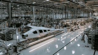
The building itself is almost modest: two steel-frame stories, roughly 1,100 square meters of floor area on a 5,800-square-meter site, with five clean rooms inside. Production equipment will move in over the coming year, and the plant is meant to reach full operation around fiscal 2028, eventually able to turn out several hundred thousand diamond chips a year. The company hasn't disclosed what it spent.
The numbers that matter most are smaller and more human. Okuma was an evacuation zone after the accident; rebuilding a community there means jobs. The company plans to hire about 20 people this fiscal year and more than 40 by 2028, with a deliberate emphasis on local recruitment. Its first products are aimed straight at the reactor that defined the town: radiation-hardened devices for analyzing and extracting fuel debris, starting with a diamond-chip neutron detector.
What makes the factory plausible rather than aspirational is what came before it. Across a decade of decommissioning work, the team built what it describes as the world's only fully vertical manufacturing chain for diamond chips, from substrate design to the finished amplifier, and reached a yield above 90 percent at lab scale. Those ten years did something else, too: they put the company in constant conversation with the people who would actually buy the technology, which is usually the part deep-tech startups get wrong.
What comes after the reactor
If diamond chips only ever served the Fukushima cleanup, they would still matter. But the company is clear that the reactor is a beginning, not a ceiling.
The same toughness that survives a reactor core is exactly what satellites, defense radar, and the power-hungry base stations of post-5G and 6G networks are starving for: high power and high frequency packed into something small that doesn't melt. And Japan happens to be unusually strong in precisely the power-semiconductor industry where diamond's edge is largest, with Mitsubishi Electric, Fuji Electric, Toshiba and Rohm all among the global leaders. The downstream industry that could put these chips to work, in other words, is already in place at home.
There's a Japanese word that hangs over all of this: fukko. It's usually rendered as "reconstruction," but the translation undersells it. The word carries less the sense of returning things to how they were than of growing something that was never there before, up out of the wreckage. A plant turning out the world's most advanced semiconductor, in the shadow of the reactor that nearly broke the region, is about as concrete as that idea ever gets.
Has a crisis in your country ever produced something nobody saw coming?
References
- https://news.yahoo.co.jp/articles/172a8490fb10e564d49096544a387c39c4160613
- https://ookuma-dd.com/brandstory/
- https://ookuma-dd.com/company/
- https://www.nippon.com/en/news/yjj2026052900988/diamond-semiconductor-plant-completed-in-northeastern-japan.html
- https://www.japan.go.jp/kizuna/2025/02/diamond_semiconductors.html
- https://coralcap.co/2026/04/japans-apollo-moment-diamond-semiconductors/?lang=en






Global Discussion
0 comments