🌡️ Common sense says you cool a supercomputer with the coldest water possible. Japan's Fugaku NEXT, set to launch around 2030, throws that out the window: it will deliberately use water warmer than 30°C (86°F) to cool its CPUs and GPUs. And on the memory side, SoftBank and Intel are joining forces on a chip that stands DRAM dies on edge and connects them through magnetic fields, aiming to leapfrog the dominant HBM standard. While the US races toward gigawatt-scale "throw electricity at it" AI machines, why is Japan zigging where everyone else zags?
A Strategic Pivot: From "World's Fastest" to "Most Used"
The next-generation supercomputer "Fugaku NEXT," co-developed by Japan's RIKEN research institute, Fujitsu, and US chip giant NVIDIA, finished the basic architectural design in March 2026 and moved into detailed design, its first real milestone toward a 2030 launch.
What's striking is how dramatically the design philosophy has shifted from its predecessor. The original Fugaku captured the #1 spot on the global TOP500 supercomputer ranking in June 2020 and held it for four consecutive periods, a source of immense national pride in Japan.
Fugaku NEXT, by contrast, openly states it is not chasing the world #1 ranking. Instead, the goal is to deliver up to 100 times the application performance of Fugaku, meaning real-world scientific computing throughput, not synthetic benchmark scores, while limiting the increase in power consumption to roughly 30 percent. In an era when AI is causing supercomputer power budgets to balloon, RIKEN is betting on efficiency and "computers people actually use" instead of trophy machines.
Counterintuitive Move #1: Cooling With Warm Water Instead of Cold
The first surprise is the cooling system.
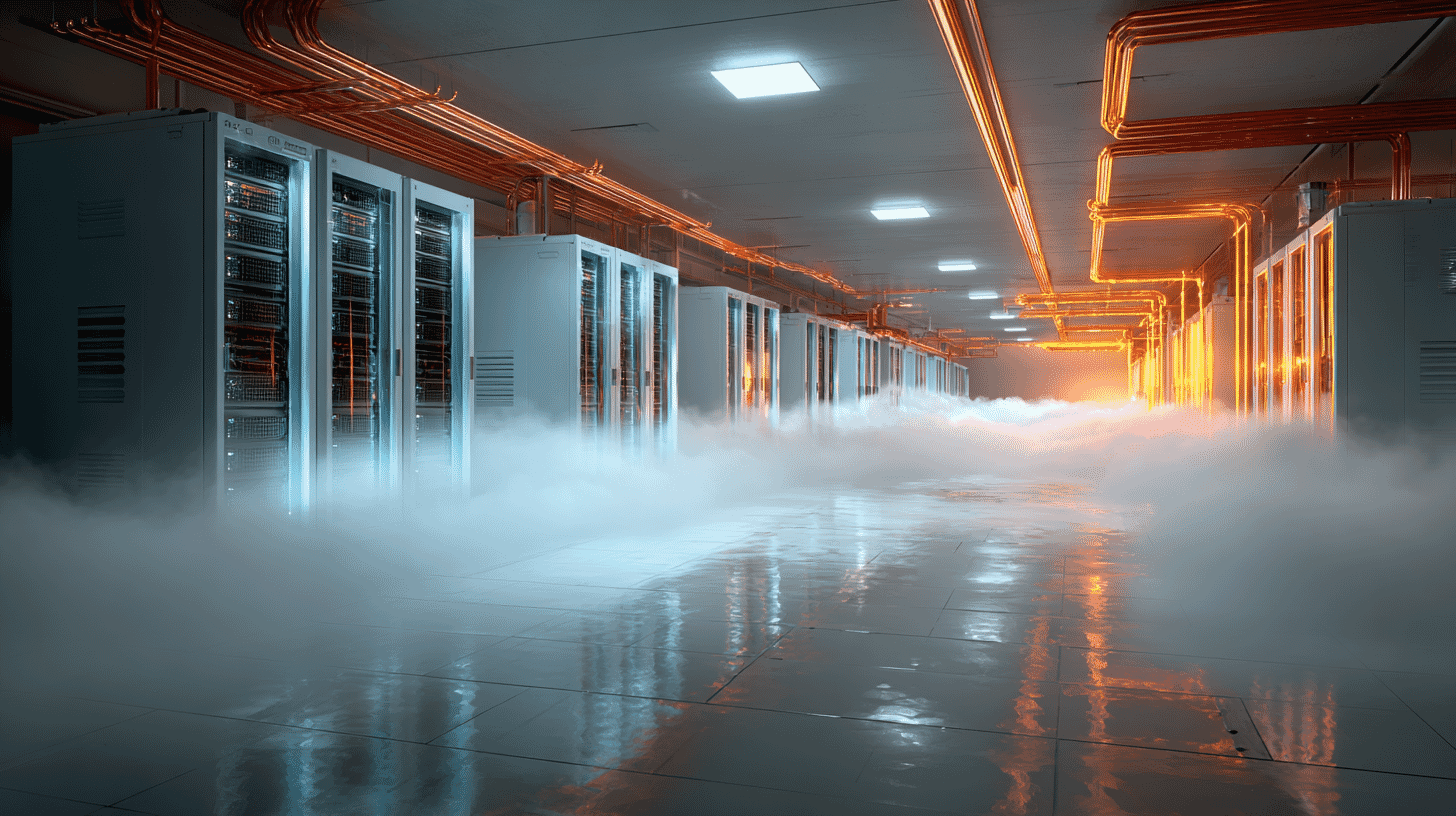
The current Fugaku circulates roughly 15°C (59°F) cold water through heat sinks pressed against each CPU. Next door to the computer hall sits a machinery building packed with industrial chillers running 24/7 to produce that cold water, a major electricity draw in itself. Fugaku uses about 17 megawatts for computation, and its annual electricity bill including cooling runs to roughly ¥5 billion.
Fugaku NEXT scraps this approach. Servers will instead be cooled by water heated above 30°C (86°F), eliminating the chillers entirely. RIKEN expects this single change to cut cooling-related power consumption by about 20 percent compared with Fugaku. Shinichi Miura of RIKEN's Center for Computational Science, who leads the cooling and power infrastructure design, sums up the goal as extracting maximum compute from a constrained budget.
"Can lukewarm water really cool a CPU?" you might wonder. Modern server chips are designed to operate reliably at surface temperatures of 80–90°C, so as long as the cooling water is meaningfully cooler than that, heat removal works. The trade-off is favorable: you give up the marginal benefit of running chips at extra-cold temperatures, and in exchange you cut the entire chiller plant from your electricity bill.
There's a second benefit. Water that exits the system at over 30°C is hot enough to be reused, for building heating, or potentially exported as energy to nearby facilities. The supercomputer becomes part of a local energy loop instead of pure waste heat.
The US Is Doing the Exact Opposite: Gigawatt-Scale Power
This design philosophy stands in stark contrast to where leading US labs are heading.
The June 2026 TOP500 list was reordered by a newcomer. China's LineShine, installed at the National Supercomputing Centre in Shenzhen, debuted at #1 with 2.198 exaflops on HPL. Lawrence Livermore National Laboratory's El Capitan dropped to #2 at 1.809 exaflops, Oak Ridge National Laboratory's Frontier holds #3 at 1.353 exaflops, and Fugaku sits at #9 with 442 petaflops. Fugaku also lost its long-held crown on HPCG, the benchmark considered more representative of real industrial workloads: it now ranks third at 16.00 petaflops, behind LineShine (22.00) and El Capitan (17.41).
What comes next on the US/European roadmap is even more extreme: gigawatt-class AI supercomputers. In May 2025, NVIDIA announced an "800-volt direct current" power architecture for AI servers, in which AC power is converted to 800V DC outside the rack and delivered straight to the GPUs. The result: rack-level power densities exceeding 1 megawatt. Texas Instruments, Germany's Infineon Technologies, Japan's ROHM and Renesas, Hitachi, and France's Schneider Electric have all signed on as ecosystem partners.
Fugaku NEXT plans to skip 800V DC, citing both engineering trade-offs and Japan-specific regulatory hurdles: the country's electrical safety standards were not written with high-voltage DC distribution in data centers in mind. It is an explicit decision to pass on what is becoming the global default.
Counterintuitive Move #2: Memory Chips That Stand on Edge
The memory choice is just as unconventional.
Modern AI servers are built around a memory technology called HBM (High Bandwidth Memory), which stacks DRAM dies vertically and connects them through "through-silicon vias" (TSVs), microscopic vertical wires drilled through each die. HBM delivers data transfer rates an order of magnitude beyond conventional DRAM and is now standard equipment alongside flagship GPUs like NVIDIA's Blackwell.
But HBM has a ceiling. Because the dies are stacked flat on top of one another, power and heat constraints cap the practical stack at roughly today's 16 layers, with around 20 seen as the limit. Production capacity is tight and AI demand has kept prices high.
Enter SAIMEMORY, a wholly owned SoftBank subsidiary established in December 2024 and up and running by mid-2025, built to design a different kind of stacked memory. It signed a collaboration agreement with Intel on February 2, 2026, and is developing ZAM (Z-Angle Memory): an architecture that stands DRAM dies on edge, perpendicular to the substrate, and connects them with a wireless magnetic-coupling I/O rather than physical wiring.
The point of the unusual geometry is heat. Standing the dies up lets each one shed heat evenly upward, loosening the layer-count limit that constrains flat stacks, and the contactless coupling targets power consumption at roughly half of current parts. SAIMEMORY president and CEO Hideya Yamaguchi has said today's memory technology will hit its limits around 2030, which is when he intends to put the company's own product on the market. The CTO is Stephen Morein, an Intel veteran.
ZAM as Japan's Memory Comeback Bet
ZAM is scheduled for a prototype in fiscal 2027 and practical deployment in fiscal 2029, conveniently aligned with Fugaku NEXT's 2030 launch window. RIKEN has signaled that if ZAM meets the specification requirements, the supercomputer will adopt it. Meanwhile, the custom CPU Fujitsu is developing for Fugaku NEXT, codenamed FUJITSU-MONAKA-X, a 1.4nm Arm-based design, is being lined up for manufacturing at Rapidus, Japan's heavily state-backed domestic foundry. If both pieces fall into place, Fugaku NEXT becomes very nearly an "all-Japan" supercomputer at the chip level, despite still relying on NVIDIA GPUs.
The investment numbers are modest by global standards. SoftBank is putting in roughly ¥3 billion (about $18 million at ¥163/USD), Fujitsu and RIKEN together about ¥1 billion (about $6 million), with additional support from Japan's Ministry of Economy, Trade and Industry. Total funding through fiscal 2027 is expected to reach about ¥8 billion (about $49 million). In April 2026 the ZAM project, run jointly by SAIMEMORY and Intel with RIKEN as a research partner, was selected for a NEDO subsidy program for advanced semiconductor manufacturing technology.
This is a meaningful moment for Japan. The country once dominated the global DRAM market in the 1980s before being squeezed out by South Korean and Taiwanese rivals starting in the 1990s. Today, Japan has zero domestic DRAM manufacturing. ZAM follows the same pattern Rapidus is following on the logic side: import US technology, add government backing, attempt domestic mass production. It is a high-stakes test of whether Japan can rebuild a strategic semiconductor sector it lost decades ago.
CPU and GPU as Partners, Not Rivals
Fugaku NEXT's third notable choice is its hybrid CPU+GPU architecture.
Today's Fugaku is essentially a CPU-only machine, packing roughly 7.6 million cores of Fujitsu's homegrown A64FX processor and adding AI-acceleration features into the CPU itself rather than relying on external GPUs. It's a distinctive, and somewhat lonely, design choice in a world that's gone all-in on GPU computing.
Fugaku NEXT abandons that approach. AI workloads will be handled primarily by NVIDIA GPUs, with Fujitsu's MONAKA-X handling secure processing and power-efficient workloads. This represents a major philosophical shift, from "Japanese sovereign supercomputer that goes its own way" to "pragmatic coexistence with NVIDIA's dominant ecosystem." Where past Japanese national projects often emphasized independence almost as an end in itself, Fugaku NEXT picks its battles.
Why Japan Chose the Efficiency Path
So why is Japan zigging while the US zags toward gigawatt-scale brute force?
First, electricity economics. Japanese industrial electricity prices run roughly 2–3 times those in the US, with limited renewable capacity and grid headroom. The American assumption of "we'll just buy more power" is simply not viable in Japan.
Second, mission profile. Frontier and El Capitan exist primarily to run nuclear weapons stockpile simulations and similar national-security workloads where peak performance justifies almost any electricity bill. Fugaku NEXT, by contrast, is being optimized for industrial use, drug discovery, climate modeling, and AI inference, workloads run every day, where electricity costs accumulate visibly on someone's budget.
Third, industrial policy. Combining domestic technologies like MONAKA-X and ZAM into one flagship system is a way to seed a "Made in Japan" data-center hardware ecosystem. Building one trophy machine matters less than producing efficient technology that can be sold at scale into commercial data centers, which is where the real economic returns live.
Fugaku NEXT's fiscal 2025 budget was about ¥7.3 billion (roughly $45 million). The total has not been fixed, but is widely expected to exceed ¥100 billion (over $600 million), in line with what the K computer and Fugaku each cost. That's a fraction of comparable US flagship investments, and that's the entire point: Japan is deliberately declining to outspend anyone.
Risks and Open Questions
The strategy isn't without risks.
SAIMEMORY remains a small organization, reportedly fewer than a few dozen staff, and is actively recruiting design engineers. Receiving Intel technology is helpful, but moving from prototype to volume production requires an entire ecosystem Japan has spent 30 years allowing to atrophy.
Warm-water cooling also faces validation challenges. As NVIDIA's GPU thermal density continues to climb generation after generation, will 30°C+ water still get the heat out fast enough? US-led teams are simultaneously pursuing immersion cooling (submerging entire servers in non-conductive fluid) as another path. The "right" answer isn't yet clear.
The CPU+GPU hybrid architecture also introduces communication bottlenecks between the two compute types. Inheriting Fugaku's distinctive Tofu interconnect technology will be critical to keeping data flowing between MONAKA-X and the NVIDIA GPUs.
Still, while the rest of the field rushes toward "throw more electricity at the problem," Japan choosing "warm water and magnetic coupling" matters. AI infrastructure may not converge on a single optimal answer, and having genuinely different architectures in the world is, ultimately, useful for everyone.
In Japan, Fugaku NEXT's "efficiency over scale" message is increasingly seen as a coherent philosophy for AI infrastructure in an energy-constrained future. What's the conversation like in your country? Are AI data center power consumption and cooling getting public attention where you are? And which do you think should win, efficiency, or raw scale?
References
- https://xtech.nikkei.com/atcl/nxt/column/18/03549/041600003/
- https://www.nikkei.com/prime/tech-foresight/article/DGXZQOUC224IF0S6A420C2000000
- https://xtech.nikkei.com/atcl/nxt/column/18/00001/11484/
- https://xtech.nikkei.com/atcl/nxt/column/18/00001/11457/
- https://sj.jst.go.jp/news/202512/n1223-01p.html
- https://top500.org/news/el-capitan-achieves-top-spot-frontier-and-aurora-follow-behind/
- https://www.r-ccs.riken.jp/fugaku/facility/







Global Discussion
14 comments